
Abstract:The impedance characteristics of distributed amplifiers are analyzed based on T-type matching networks, and a distributed power amplifier consisting of three gain cells is proposed. Non-uniform T-type matching networks are adopted to make the impedance of artificial transmission lines connected to the gate and drain change stage by stage gradually, which provides good impedance matching and improves the output power and efficiency. The measurement results show that the amplifier gives an average forward gain of 6 dB from 3 to 16.5 GHz. In the desired band, the input return loss is typically less than -9.5 dB, and the output return loss is better than -8.5 dB. The output power at 1-dB gain compression point is from 3.6 to 10.6 dBm in the band of 2 to 16 GHz while the power added efficiency (PAE) is from 2% to 12.5%. The power consumption of the amplifier is 81 mW with a supply of 1.8 V, and the chip area is 0.91 mm×0.45 mm.
Key words:distributed amplifier; impedance matching; power added efficiency; T-type network
With the rapid development of wireless and optical communications, the continuous increase in the data transfer rate requires amplifiers with wider bandwidths. Distributed amplifiers (DAs) provide an effective solution for extending the bandwidth and, therefore, are widely used in the design of ultra-high broadband systems.
Recently, many distributed amplifiers have been designed and realized by advanced process technologies, such as GaAs PHEMT technology[1-3], SiGe BiCMOS technology[4-5] and AlGaN/GaN HEMT technology[6-7], which show great amplification and frequency performance. Conversely, the CMOS technology is relatively inferior but still acceptable in practical applications, and it makes itself more competitive than those advanced process technologies due to its much lower price.
This paper presents a distributed power amplifier based on the impedance matching of T-type networks. The chip is fabricated with the standard 0.18-μm CMOS technology of SMIC. The measurement results show that the amplifier obtains an average gain of 6 dB in the band of 3 to 16.5 GHz. The output power at 1-dB compression point (P1-dB) is from 3.6 to 10.6 dBm in the band of 2 to 16 GHz, while the power added efficiency (PAE) is from 2% to 12.5%. The power consumption is 81 mW with the supply of 1.8 V, and the chip area is 0.91 mm×0.45 mm.
In DAs, the parasitic capacitances of transistors are combined with on-chip inductors to construct the artificial transmission lines, and the gain roll-off due to the parasitic capacitances of transistors is reduced. The classical circuit of DAs is shown in Fig.1. If the loss of artificial transmission lines is neglected, the corresponding equivalent circuits are shown in Fig.2. The signal phase delay of artificial transmission lines in the gate and drain should be matched so that the signals in different paths are added positively to the output port.
Traditionally, the transmission line theory is the basis of the design of DAs. According to this theory, the voltage gain Av and the characteristic impedance Z0 of DAs (not considering the loss of artificial transmission lines) are given as
(1)
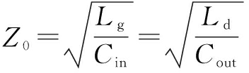
(2)
where Z0 is normally set to be 50 Ω; Cin and Cout are the input and output parasitic capacitance of gain cells, respectively; Lg and Ld are the on-chip inductor of artificial
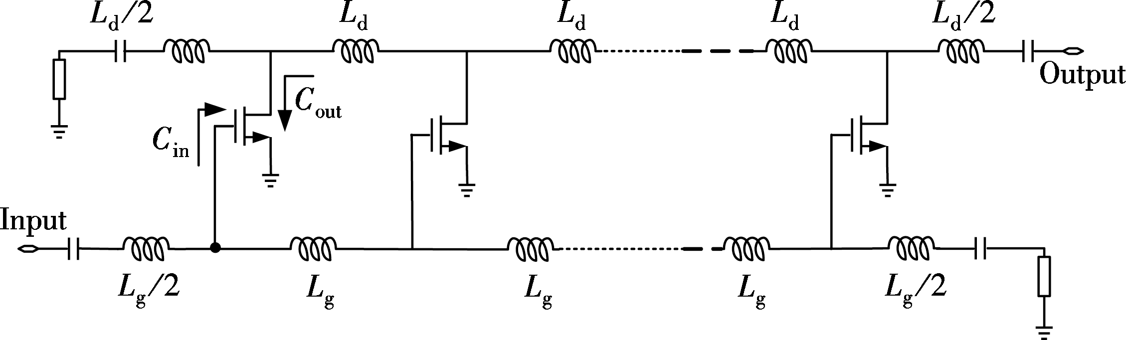
Fig.1 Classical distributed amplifier
(a)

(b)Fig.2 Equivalent artificial transmission lines. (a) Gate; (b) Drain
transmission lines in the gate and drain, respectively. The desired inductance can be calculated according to Eq.(2) if the parasitic capacitance of transistors is known.
The bandwidth of distributed amplifiers is mainly restricted by the cutoff frequency fc of artificial transmission lines:
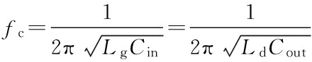
(3)
According to Eq.(2), Lg and Ld are proportional to Cin and Cout when the characteristic impedance is fixed. From Eq.(3), the cutoff frequency fc decreases with the increase of Lg (Ld) and Cin (Cout). So, the contradiction between the gain and the bandwidth still exists in DAs, which is much more serious in conventional amplifiers.
From Fig.2, the gate and drain artificial transmission lines consist of T-type networks, so the input and output impedance of DAs should change with the values of on-chip inductors. To conduct the operation, the artificial transmission line constructed by four stages of T-type network is selected as an example and the parasitic capacitance of transistors is set to be 80 fF. Fig.3 shows how the return loss of the artificial transmission line changes with the on-chip inductor L. In Fig.3, 160 pH is a good choice for the impedance matching in the band below 22 GHz while 240 pH is better for the band from 22 to 54 GHz. This cannot be explained clearly using the transmission line theory.
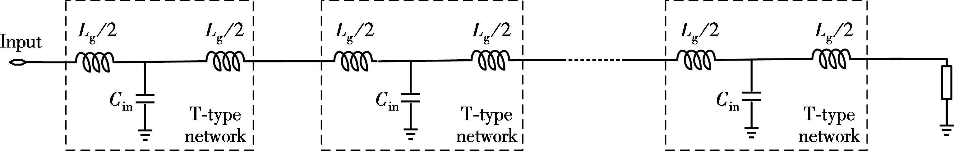
The artificial transmission lines in DAs can be regarded as the cascaded network which is composed of a T-type network, as shown in Fig.4. In Fig.4, C is the parasitic
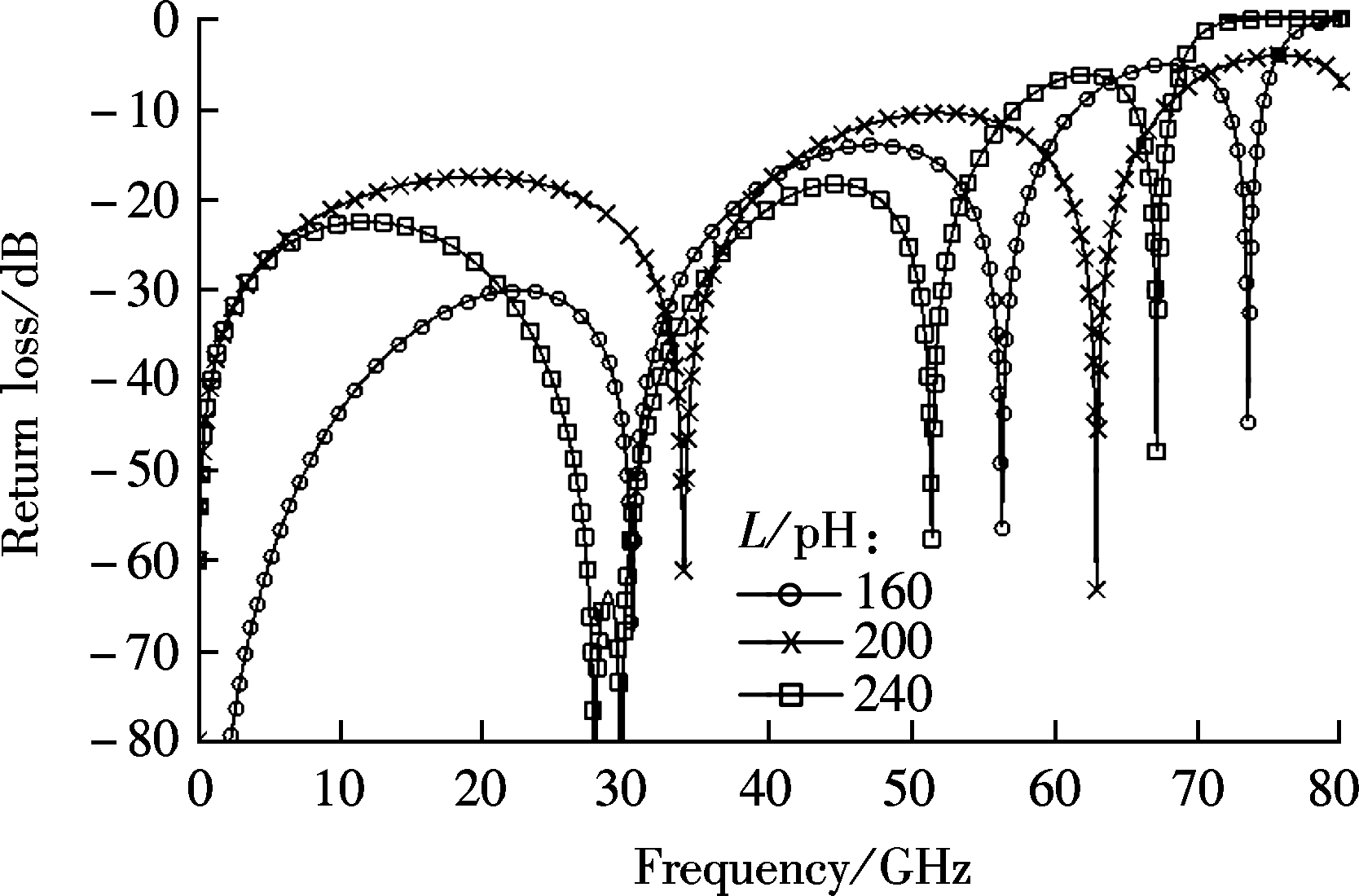
Fig.3 Return loss of the artificial transmission line
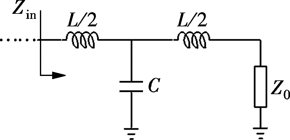
Fig.4 T-type matching network
capacitance of the gate or the drain of transistors and L is the on-chip inductor, which constructs the artificial transmission line. The input impedance Zin can be expressed as
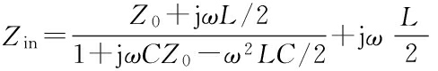
(4)
Let Zin=Z0, and the characteristic impedance Z0 is derived as
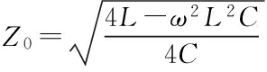
(5)
From Eq.(5), it can be shown that ![]() when ω2L2C≪4L (i.e.
when ω2L2C≪4L (i.e. ![]() ≪1), and it corresponds to the characteristic impedance in Eq.(2), which is from the transmission line theory.
≪1), and it corresponds to the characteristic impedance in Eq.(2), which is from the transmission line theory.
The impedance matching process of the T-type network in Fig.4 is shown in Fig.5. A perfect impedance matching at some frequency is obtained by the T-type network consisting of two inductors in series and one shunt capacitor, and the bandwidth of this matching network is constrained by the max quality factor at four transition points of m, n, p and q. The larger (i.e. the larger parasitic capacitance) and smaller (i.e. the smaller parasitic capacitance) quality factor is indicated by the solid line and dotted line, respectively.
A uniform distributed power amplifier is designed based on T-type network and impedance matching method. The designed amplifier is shown in Fig.6. The cascode structure with the series inductor[8] is used as the gain cell to

Fig.5 Impedance matching process of T-type network
enhance the forward gain and the reverse isolation. Considering the output power, the gain and the bandwidth in tradeoff, the gate width of transistors is set to be 120 μm.
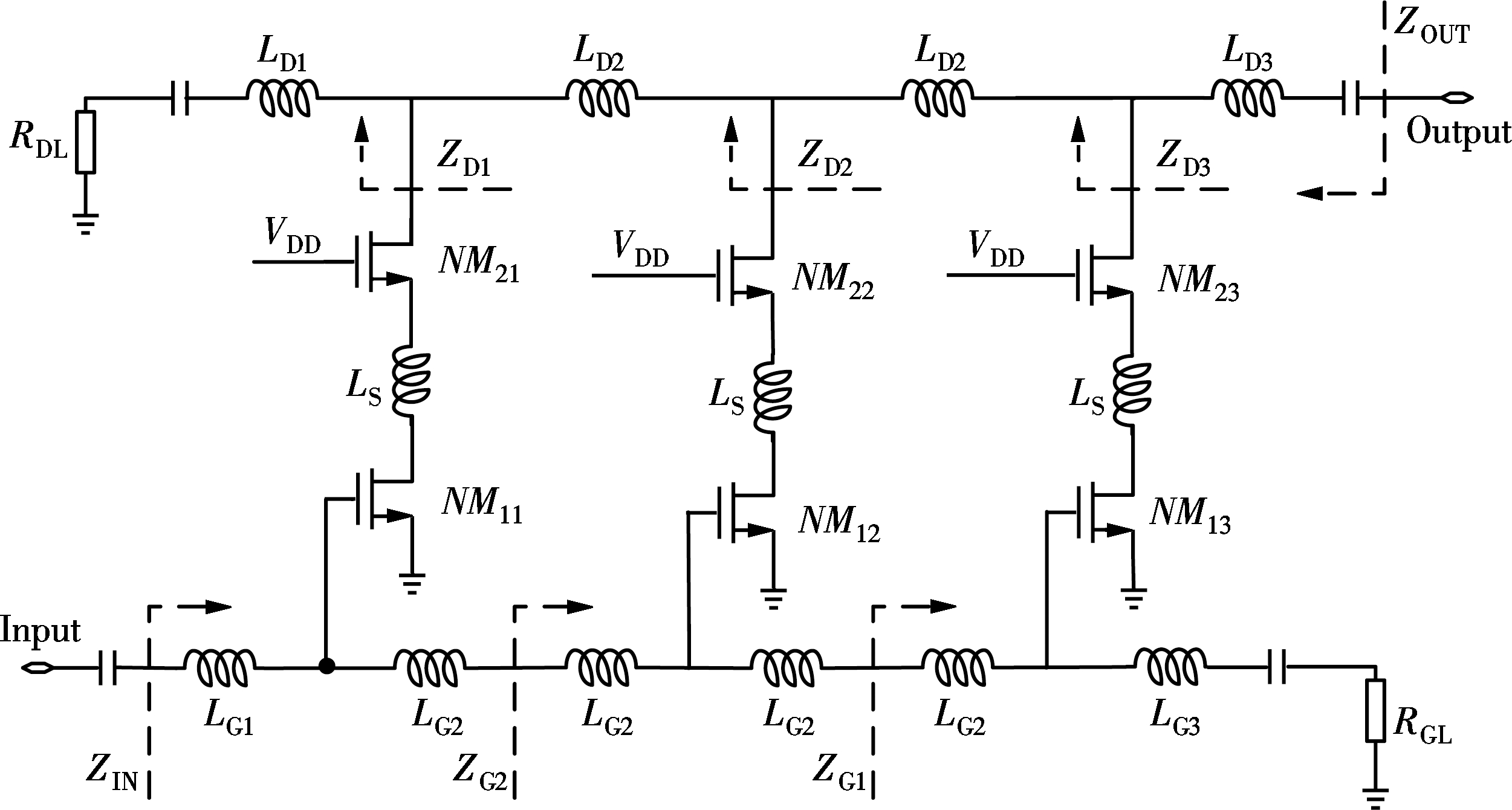
Fig.6 Designed distributed power amplifier
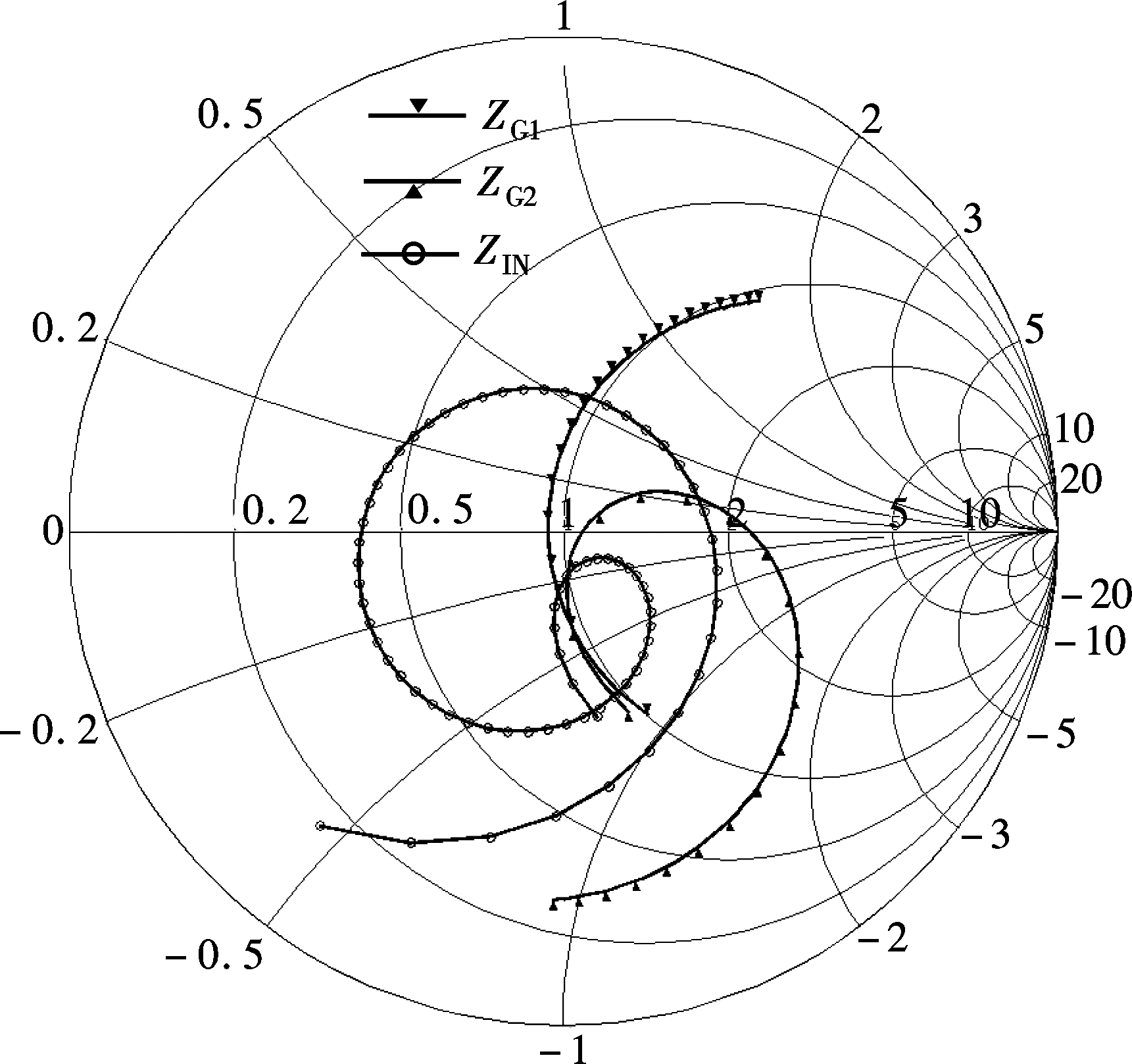
The uniform T-type networks are cascaded at the gate artificial transmission line except at the first stage, of which the first series inductor LG1 is set a little larger to match the parasitic capacitance of the input pad. The impedance at different points of the cascade T-type networks is shown in Fig.7. Fig.7 shows that the impedance changes around 50 Ω with the increase in the number of cascade T-type networks in the wide band, which is similar to the impedance transformation characteristics of transmission lines. But the curve of impedance is not a perfect circle because of the unexpected loss of transistors and on-chip inductors, which makes the design more complex. Hence, the load resistor of the gate artificial transmission line is set to be 58 Ω instead of 50 Ω to obtain better input impedance matching.
As for the design of the drain artificial transmission line, the tradeoff between the output power and the impedance matching should be considered carefully. The design target is to find the optimum load of each gain cell and use non-uniform T-type matching networks to construct the optimum load. Fig.8 shows the load impedance of each gain cell, i.e. ZD1, ZD2 and ZD3, and they all include the output impedance of the gain cell itself. With the output signal of each gain cell increasing, the output power is mainly constrained by the output voltage swing. It is apparent that more output power can be obtained by a smaller load for the same voltage swing. In Fig.8, the increasing trend of impedance at different output points of each gain cell is presented, and the impedance approaches 50 Ω near the output port. Unlike the design methods in Refs.[7,9], the load resistor of the drain artificial transmission line is maintained and set to be 94 Ω to achieve the balance between the output power and impedance matching.
(a) 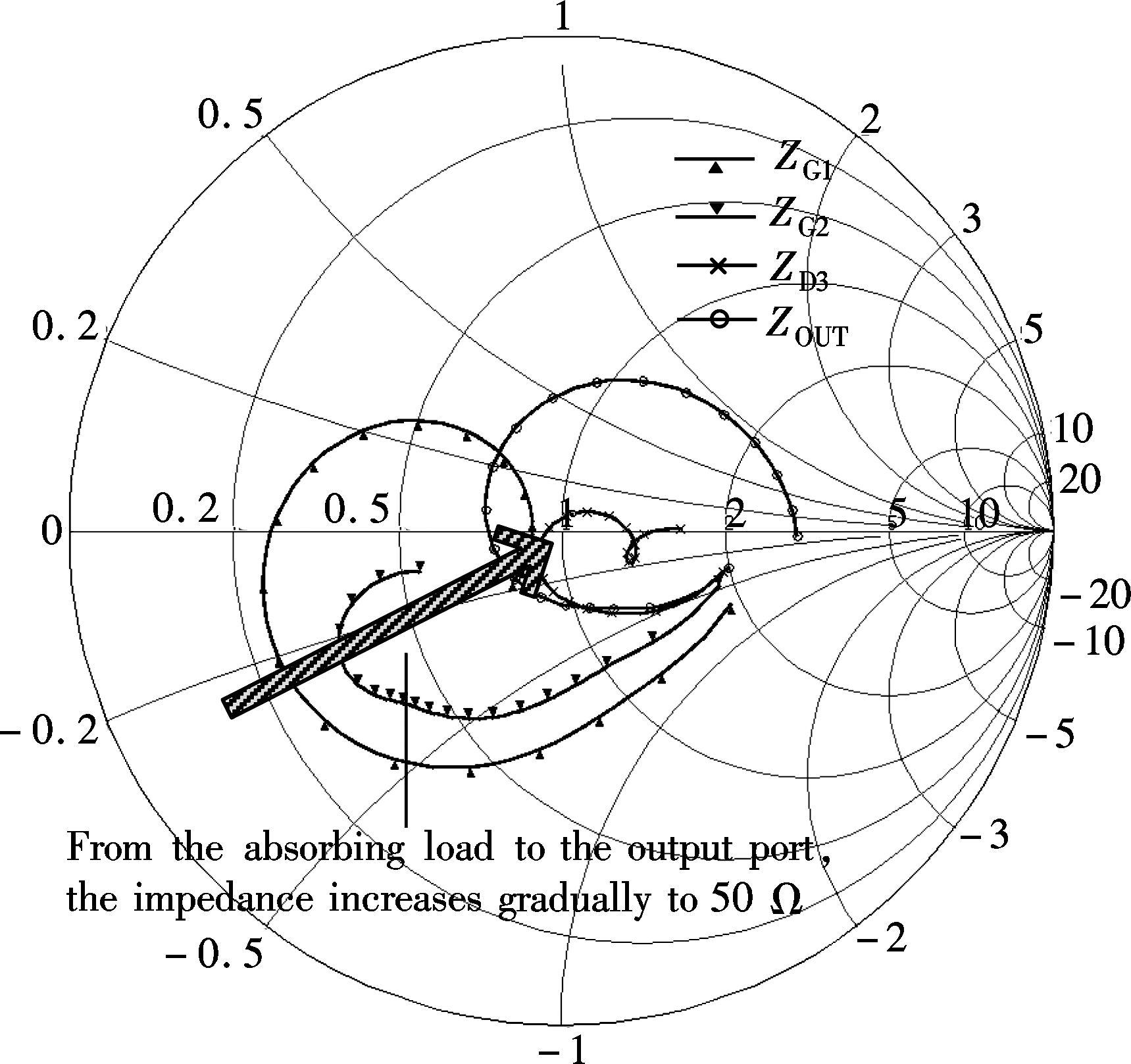 (b)
(b)
Fig.7 Impedance at different points of artificial transmission lines (1 to 16 GHz). (a) Gate; (b) Drain
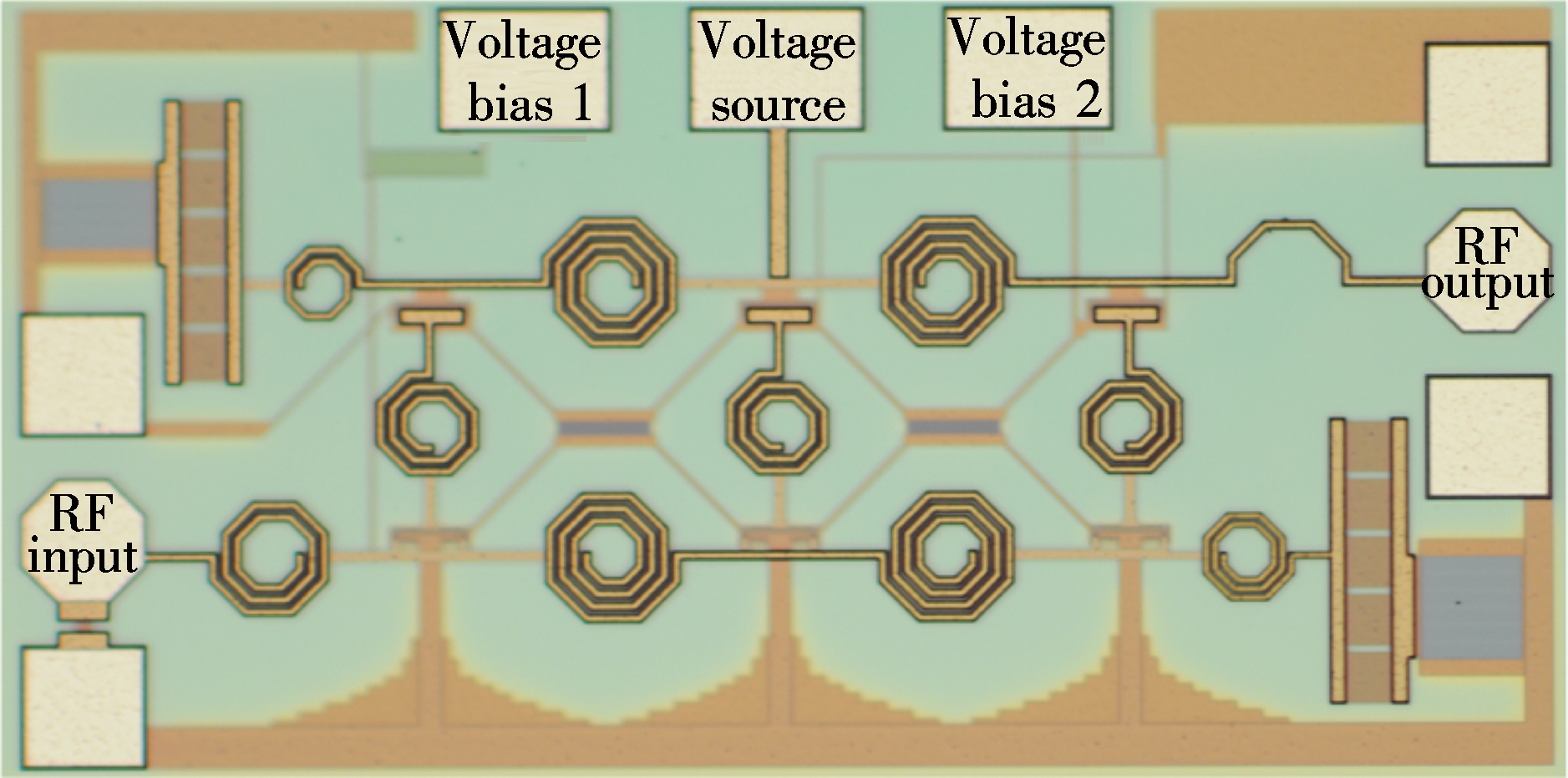
Fig.8 Die photograph
The sizes of the key devices are optimized and listed in Tab.1. The on-chip inductors are fabricated with the top metal interconnection and verified by electromagnetism simulation.
Tab.1 Sizes of the key devices
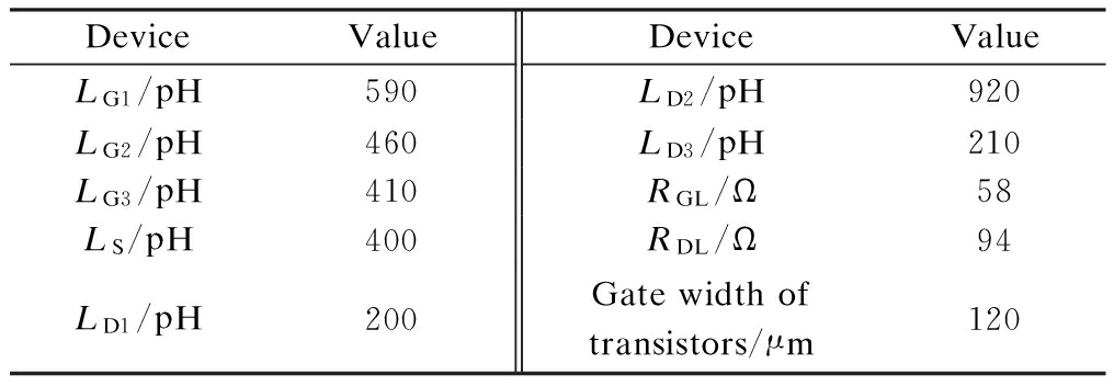
DeviceValueDeviceValueLG1/pH590LD2/pH920LG2/pH460LD3/pH210LG3/pH410RGL/Ω58LS/pH400RDL/Ω94LD1/pH200Gatewidthoftransistors/μm120
The photograph of the designed distributed power amplifier is shown in Fig.8. The area of the die is 0.91 mm×0.45 mm. The circuit is measured via on-wafer test. The measurements were carried out using an Agilent E8363B vector network analyzer, an E8257D vector signal generator and an E4448A spectrum analyzer.
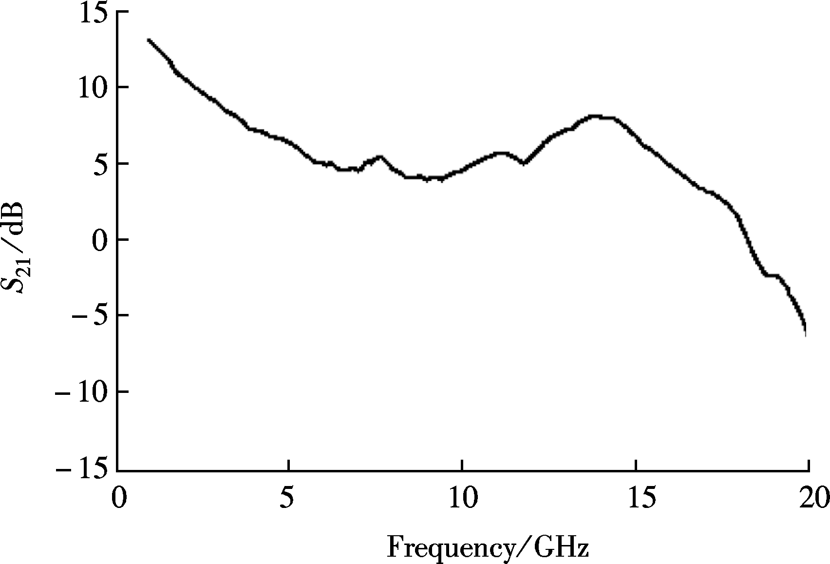
The curves without circular markers in Fig.9 give the post simulation results of S parameters while the measurement results are shown in Fig.10. The simulated forward gain (S21) is 8 dB from 2 to 14 GHz with the gain flatness of ±1 dB while the measured is 6 dB from 3 to 16.5
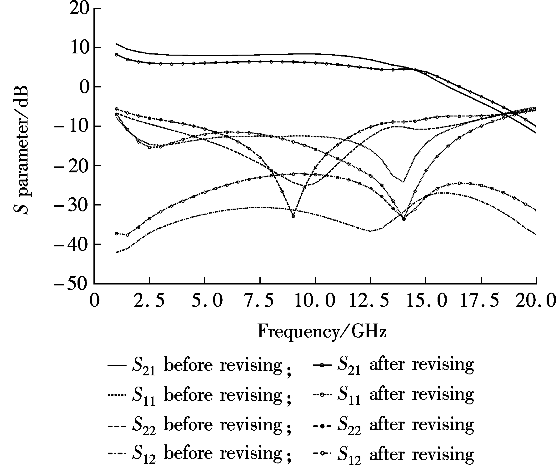
Fig.9 Simulated S parameters
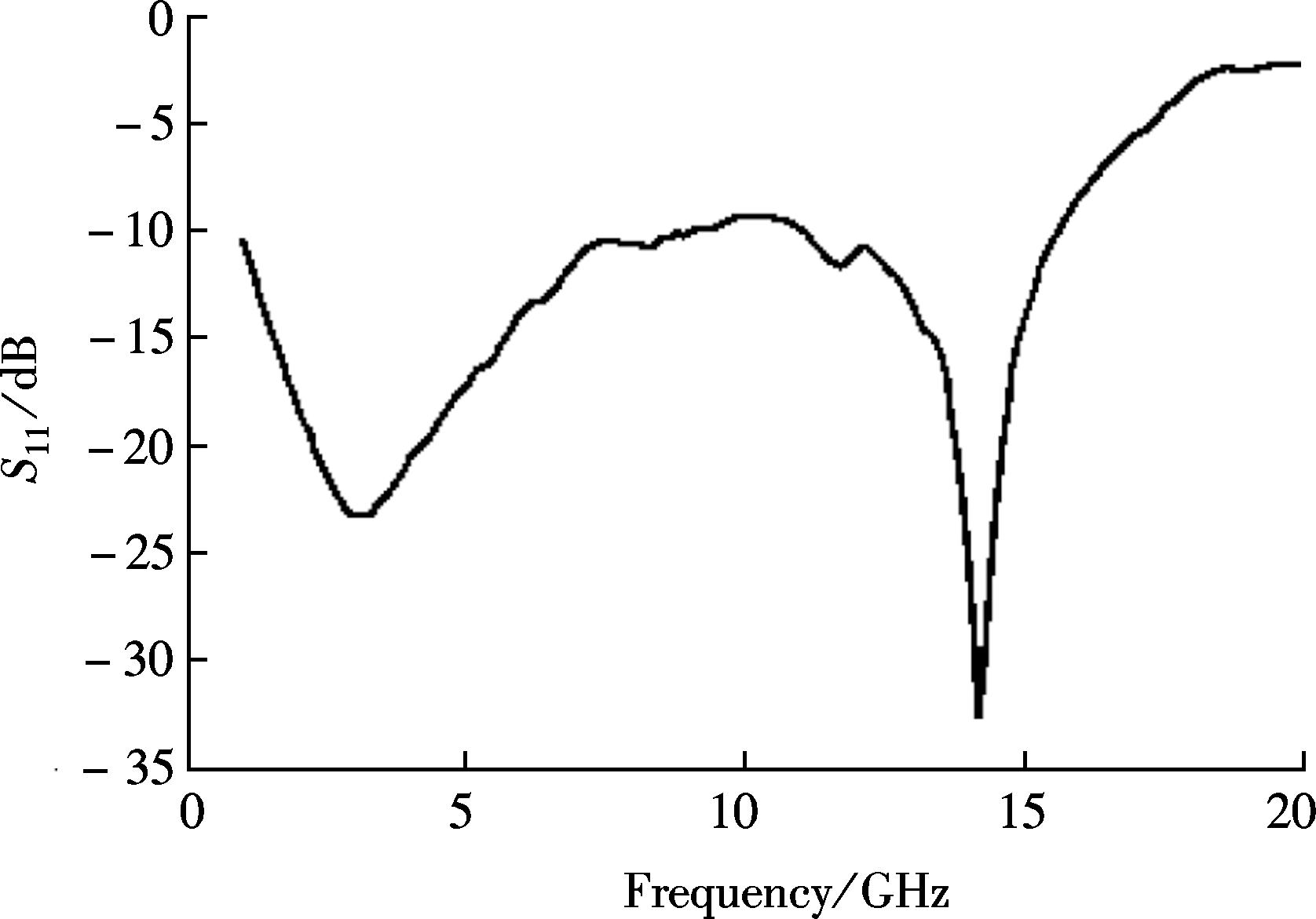
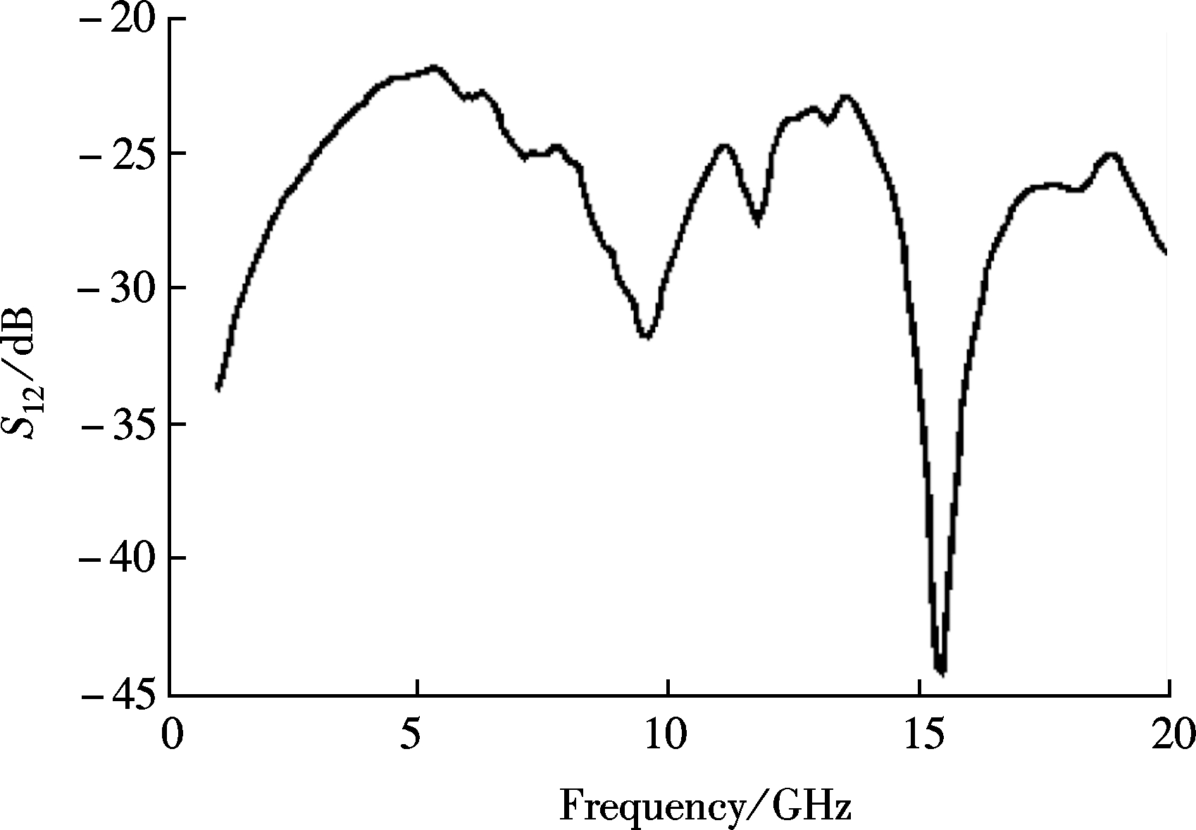
GHz with the gain flatness of ±2 dB. In the desired band, the simulated input return loss (S11) is less than -13 dB while the measured is less than -9.5 dB, and the simulated output return loss (S22) is typically less than -9 dB while the measured is less than -8.5 dB. The designed distributed power amplifier shows good power performance, which is shown in Fig.11. The output power at P1-dB is from 3.6 to 10.6 dBm in the band of 2 to 16 GHz while the PAE is from 2% to 12.5%.
Fig.9, Fig.10 and Fig.11 show that there is some inconsistency between the measured and simulated results, particularly in the high frequency band. One reason is the precision of device models. For example, the available frequency of RF NMOS transistors is lower than 10.1 GHz according to the process design kit (PDK) documents. The other reason is that the precision of the modeling of on-chip inductors may be not so good. Fig.12 shows the test structure of the on-chip inductor of 920 pH, which uses the open-short de-embedding method. The simulated and measured results are presented in Fig.
(a)
(b)
(c)
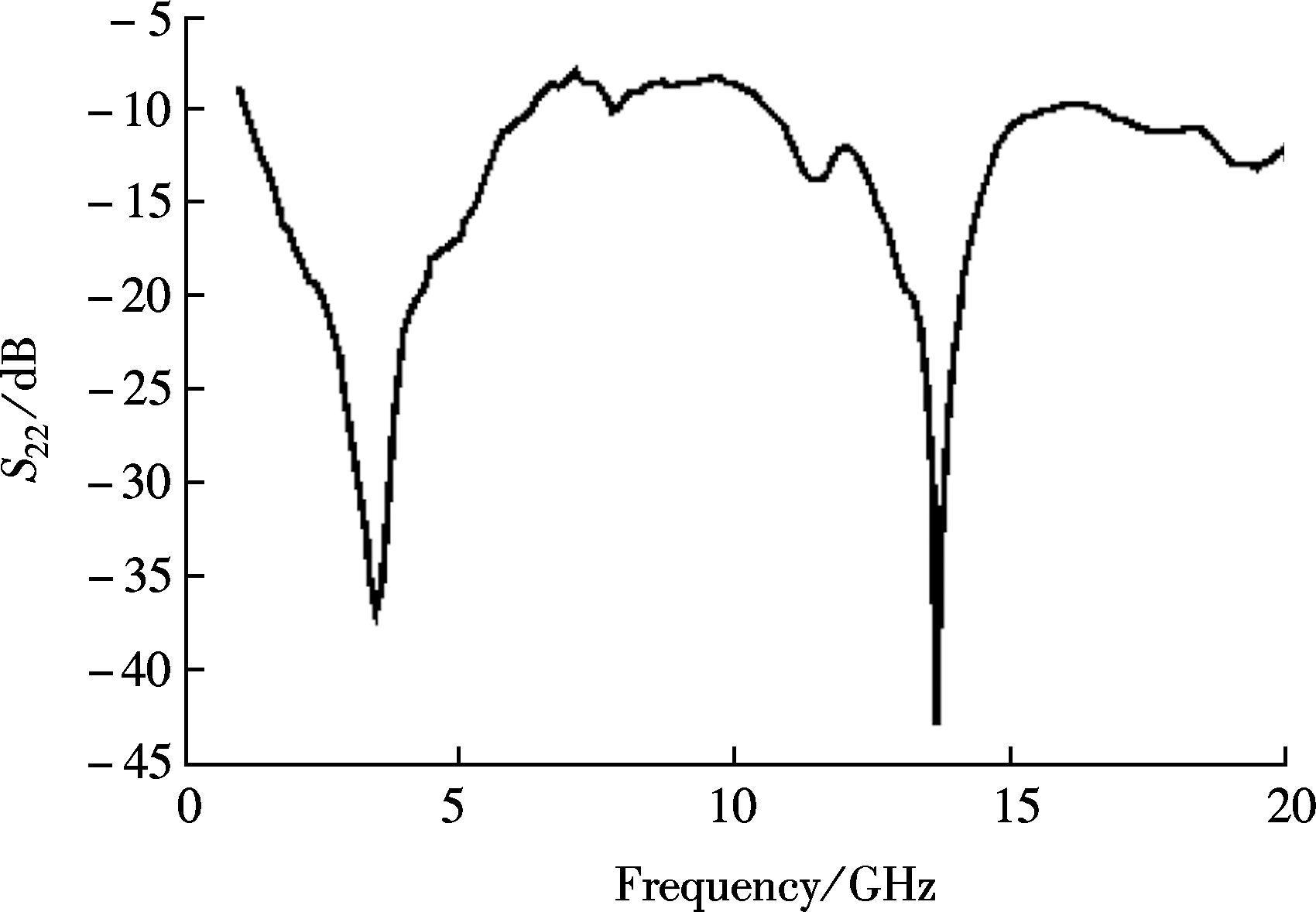
(d)Fig.10 Measured S parameters. (a) S11; (b) S21; (c) S12; (d) S22
13 and Fig.14, from which we can see that the value of the fabricated on-chip inductor is approximately 100 pH lower than the simulated one and the measured quality factor is reduced by half. The changed inductance and
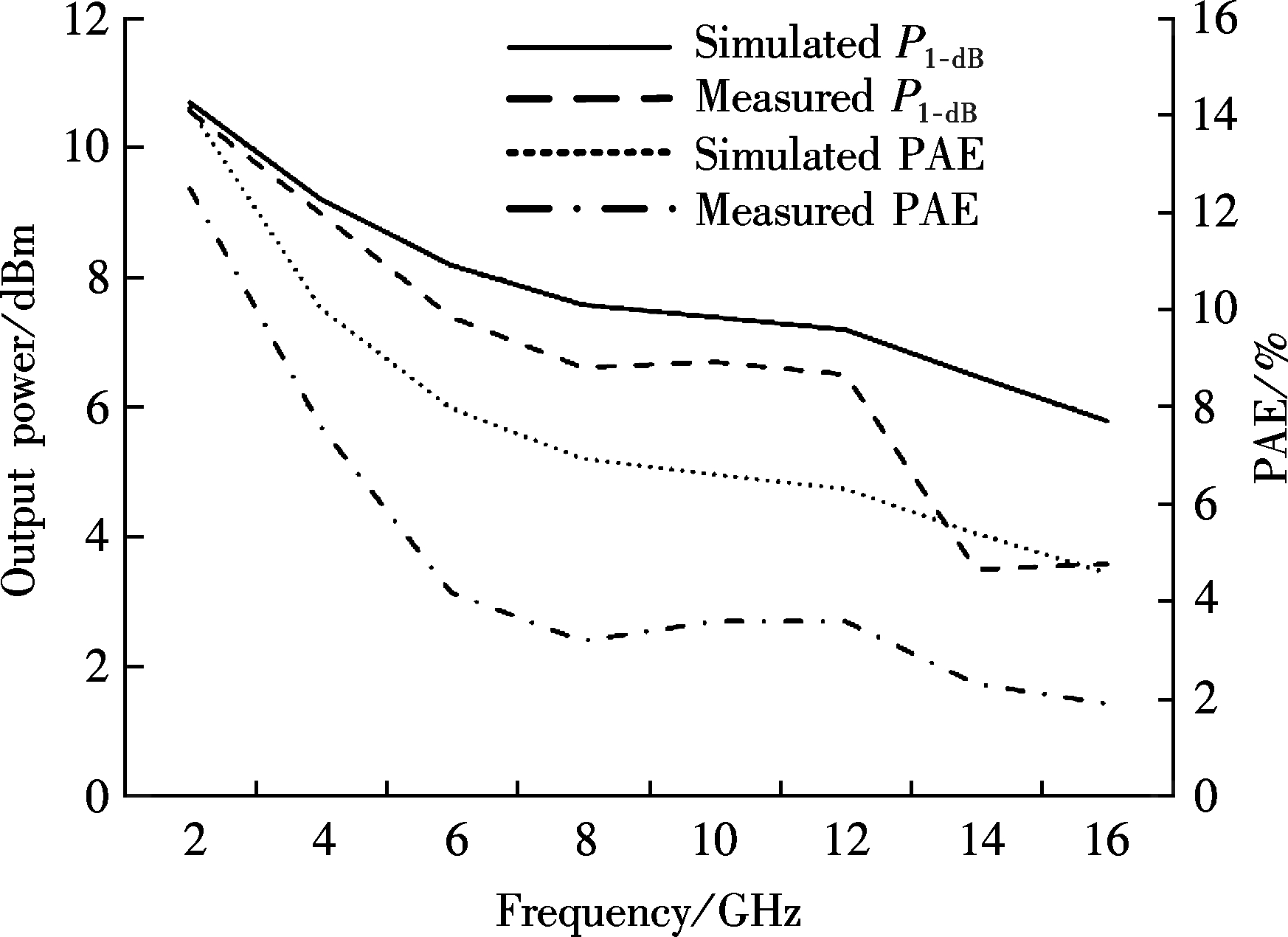
Fig.11 Comparison of the measured and simulated P1-dB and PAE
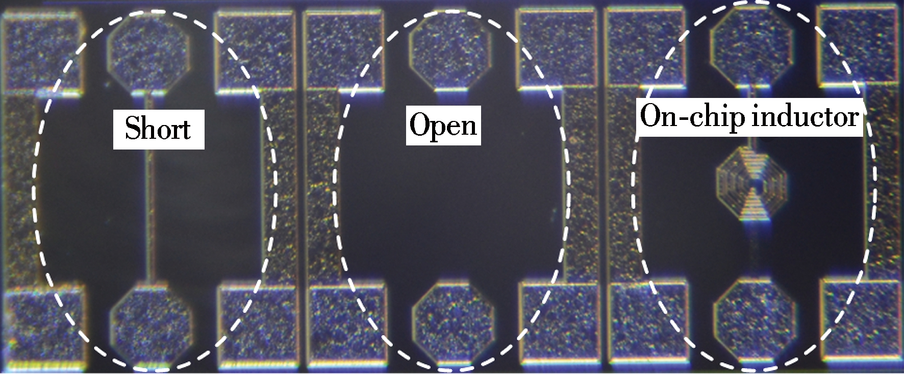
Fig.12 Test structure of on chip inductors

Fig.13 Comparison of the measured and simulated inductance
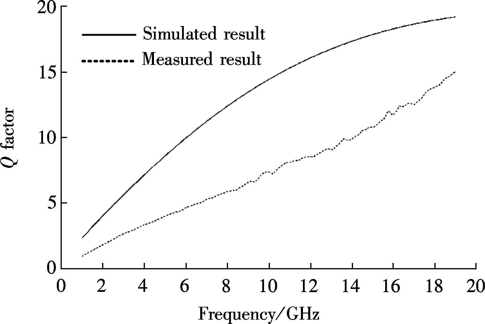
Fig.14 Comparison of the measured and simulated Q factor
parasitic resistance also change the impedance of the artificial transmission lines and the performance of the amplifier.
The parameters of some on-chip inductors are revised according to the measured results, and the corresponding curves of the post simulation results are shown in Fig.9, which are with circular markers. It is clear that forward gain S21 after revision reduces by approximately 2 dB in the band below 13 GHz, and is closer to the measured result. Also, the reverse isolation S12 after revision shows an increase of 3 to 10 dB and is more consistent with the measured S12.
The comparison between the performance of the designed distributed power amplifier and others is shown in Tab.2. Advanced technology such as GaAs PHEMT or GaAs HBT provide excellent performance in output power and efficiency, but with more area and at a much higher price. By contrast, the CMOS technology can give acceptable power performance at a much lower price. Compared with the distributed amplifier proposed in Ref.[8], the designed distributed power amplifier increases the output power by 1 dB and improves the PAE by 2.5 times at 5 GHz with half of the area, while the gain and bandwidth are reduced by 18 dB and half, respectively, as a compromise.
Tab.2 Comparison with previous reports of DAs
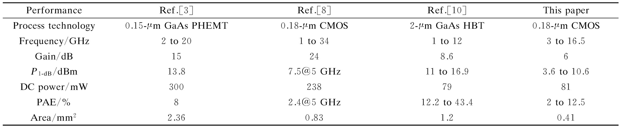
PerformanceRef.[3]Ref.[8]Ref.[10]ThispaperProcesstechnology0.15-μmGaAsPHEMT0.18-μmCMOS2-μmGaAsHBT0.18-μmCMOSFrequency/GHz2to201to341to123to16.5Gain/dB15248.66P1-dB/dBm13.87.5@5GHz11to16.93.6to10.6DCpower/mW3002387981PAE/%82.4@5GHz12.2to43.42to12.5Area/mm22.360.831.20.41
In this paper, a distributed power amplifier of three stages is presented based on SMIC 0.18-μm CMOS technology. In the design, the impedance characteristic of distributed amplifiers is analyzed based on T-type networks consisting of lumped components. The experimental results show that the designed distributed power amplifier provides good impedance matching, high output power and efficiency, which demonstrates the effectiveness of the proposed design method.
Acknowledgment The authors would like to thank Mr. Li Wei for his support on the measurement, and officers at the Institute of RF-& OE-ICs of Southeast University for the testing environment.
References:
[1]Nikandish G, Medi A. Unilateralization of MMIC distributed amplifiers [J]. IEEE Transactions on Microwave Theory and Techniques. 2014, 62(12): 3041-3052. DOI:10.1109/tmtt.2014.2361341.
[2]Kim J, Kim Y, Lee S, et al. A broadband power-reconfigurable distributed amplifier [C]//IEEE MTT-S International Microwave Symposium Digest. Montreal, Canada, 2012: 1-3.
[3]Zhang Y, Wang Z G, Xu J, et al. Design of a low noise distributed amplifier with adjustable gain control in 0.15 μm GaAs PHEMT [J]. Journal of Semiconductors, 2012, 33(3): 035003-1-035003-4. DOI:10.1088/1674-4926/33/3/035003.
[4]Chen J S, Niknejad A M. Design and analysis of a stage-scaled distributed power amplifier [J]. IEEE Transactions on Microwave Theory and Techniques, 2011, 59(5): 1274-1283. DOI:10.1109/tmtt.2011.2125985.
[5]Kim K, Nguyen C. A concurrent Ku/K/Ka tri-band distributed power amplifier with negative-resistance active notch using SiGe BiCMOS process [J]. IEEE Transactions on Microwave Theory and Techniques, 2014, 62(1): 125-136. DOI:10.1109/tmtt.2013.2292673.
[6]Dennler P, Quay R, Bruckner P, et al. Watt-level non-uniform distributed 6-37 GHz power amplifier MMIC with dual-gate driver stage in GaN technology [C]//IEEE Topical Conference on Power Amplifiers for Wireless and Radio Applications. Newport Beach, USA, 2014: 37-39.
[7]Zhou X, Roy L, Amaya R E. 1 W, highly efficient, ultra-broadband non-uniform distributed power amplifier in GaN [J]. IEEE Transactions on Wireless Components Letters, 2013, 23(4): 208-210. DOI:10.1109/lmwc.2013.2250270.
[8]Kao J-C, Chen P, Huang P-C, et al. A novel distributed amplifier with high gain, low noise, and high output power in 0.18-μm CMOS Technology [J]. IEEE Transactions on Microwave Theory and Techniques, 2013, 61(4): 1533-1542.
[9]Ersoy E, Chevtchenko S, Kurpas P, et al. A compact GaN-MMIC non-uniform distributed power amplifier for 2 to 12 GHz [C]//German Microwave Conference. Aachen, Germany, 2014: 1-3.
[10]Xu J, Wang Z G, Zhang Y, et al. High-efficiency tapered distributed power amplifier with 2-μm GaAs HBT process [J]. Microwave and Optical Technology Letters, 2011, 53(8): 1924-1927. DOI:10.1002/mop.26126.
Citation:Zhang Ying, Ma Kaixue, Zhou Hongmin, et al. Design of a distributed power amplifier based on T-type matching networks[J].Journal of Southeast University (English Edition),2016,32(3):278-284.DOI:10.3969/j.issn.1003-7985.2016.03.004.
DOI:10.3969/j.issn.1003-7985.2016.03.004
摘要:基于T型匹配网络对分布式放大器的阻抗特性进行了分析,并设计了一个三级分布式功率放大器.设计中采用非均匀的T型匹配网络结构使得与栅极和漏极相连的人工传输线阻抗逐级渐变,实现阻抗匹配的同时提升了放大器的输出功率及效率.测试结果表明:该放大器在频带3~16.5 GHz带宽内平均增益为6 dB,输入回波损耗小于-9.5 dB,输出回波损耗小于-8.5 dB;2~16 GHz频带内的1 dB增益压缩点处输出功率达到3.6~10.6 dBm,功率附加效率为2%~12.5%.电源电压为1.8 V时放大器功耗为81 mW,芯片面积为0.91 mm×0.45 mm.
关键词:分布式放大器;阻抗匹配;功率附加效率;T型网络
中图分类号:TN43
Received:2015-12-31.
Foundation item:s:The National Natural Science Foundation of China (No.61106021), the Postdoctoral Science Foundation of China (No.2015M582541), the Natural Science Foundation of Higher Education Institutions of Jiangsu Province (No.15KJB510020), the Research Fund of Nanjing University of Posts and Telecommunications (No.NY215140, No.NY215167).
Biography:Zhang Ying(1980—), male, doctor, associate professor, zhangying@njupt.edu.cn.