
Abstract:The current blockade mechanism for λ-DNA translocation under electrical field is investigated through solid-state nanopores with different pore thicknesses. The conductance of a nanopore system mainly consists of the contribution of the pore and access region, and the latter becomes dominant when the nanopore thickness gradually decreases to atomic layer thickness. Based on the existing model of nanopore resistance, a simplified model which describes the relative current blockade during the λ-DNA translocation through the nanopores is deduced to quantitatively present the relationship between nanopore thickness and relative current blockade. Results show that the relative current blockade is effectively increased by reducing the nanopore diameter but it decreases with the decreasing nanopore thickness. A two-stage schematic is proposed to increase the relative current blockade by setting a much smaller resistance region. Experimental results show a 21.9% increase in the relative current blockade with the proposed schematic.
Key words:nanopore; DNA sequencing; relative current blockade; membrane thickness
The solid-state nanopore technique is believed to be a promising method to realize third generation DNA sequencing. The basic principle is to analyze the current blockade due to the DNA molecule’s translocation through a solid-state nanopore in electrolyte solution. It shows the advantage of detecting label free DNA molecules with high throughput and at low cost. However, it is currently hindered by two main challenges[1-3], i.e. high DNA translocation speed and low spatial resolution.
To slow down the DNA translocation speed, researchers have attempted many methods in which the DNA translocation speed is actively controlled by optical tweezers[4] or AFM tips[5] by connecting the DNA molecule chain with a polystyrene bead or tip. The electrophoretic force on DNA molecules is measured by the optical tweezers, which allows us to manipulate a single polymer back and forth through the pore at a speed of 50 nm/s with nanometer precision[6].
However, the single nucleotide discrimination has not been achieved yet due to the bottleneck on low spatial resolution. In general, there are two aspects that lead to the inability to realize single nucleotide discrimination when it comes to the limitation on spatial resolution. First, a large amount of noise is shown on the current recording as measured by electrolytes for solid-state nanopore, which shows a very low signal-to-noise ratio[7]. It has long been noted that to reduce the noise, choose the membrane material with a high dielectric constant or insert an insulated sealing polymer or coating[8-10]. The patch clamp technique has also been developed rapidly, which further promotes the noise reduction. Secondly, the tiny difference for four kinds of nucleotides now cannot be effectively reflected on the ionic current recordings. In other words, one has to consider how to amplify the current variation for a DNA molecule chain translocation through a nanopore. Previously, we have presented a mini review on the methods to enhance the spatial resolution on DNA translocation through solid-state nanopores[11]. There are several novel techniques such as field effect transistors[12-13], electron tunneling[14-16], and capacitive coupling[17-19]. For these methods, the transferred electric signals are utilized for the discrimination analysis based on the ionic current change for a DNA translocation behavior, which means that the in situ current amplification technique has not been promoted. As the development in fabrication of 2D materials, it is intuitively proposed that high resolution can be acquired by decreasing the nanopore thickness to even atomic layer thickness since one current blockade peak only stands for a few nucleotides inside the ultrathin nanopore[20-22].
In this work, we provide a simple model to explain the resolution for nanopores with different thicknesses by defining the relative current blockade ΔI/I, in which ΔI stands for current change due to a DNA molecule translocation through the nanopore and I stands for the baseline current. Experimentally, the DNA translocation through both the silicon nitride nanopore and graphene nanopore is conducted to indicate the relative blockade level. Furthermore, a two-stage nanopore schematic is promoted to enhance the in situ spatial resolution.
For a typical nanopore system, the overall nanopore resistance mainly consists of two parts, i.e. pore resistance and access resistance, as shown in Fig.1(a). Once the nanopore thickness is decreased to atomic layer thickness, the resistance of the nanopore decreases and only the access resistance is left[23] as shown in Fig.1(b). Therefore, the DNA molecule blocks the ionic current on the access region when it approaches the nanopore mouth, which also leads to the ionic current variation. This means that one ionic current peak may be led to more broad area.
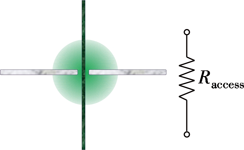
(a) (b)
Fig.1 Schematic of the resistance model.(a) Silicon nitride nanopore; (b) Graphene nanopore
The purpose of the model is to define the relative current blockade for the ultrathin nanopore, which is rarely focused on by most researchers. Some work has considered the access resistance estimation on overall resistance but ignores it when estimating the current change with DNA translocation[24]. The assumptions for this model are as follows:
1) The electrolyte solution is considered as uniform in two chambers in which 1 mol/L KCl with 10 mmol/L Tris-HCl and 1 mmol/L EDTA (pH 8.0) with a conductivity of σ (11 S/m) are filled.
2) Surface charge is not considered here to only show the physical blockade effect.
3) The electric-osmotic flow effect is not considered.
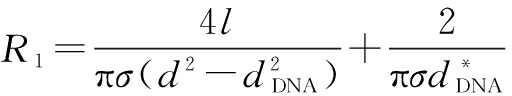
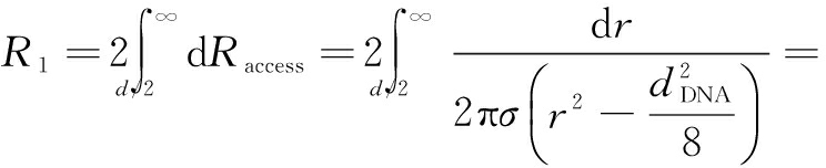
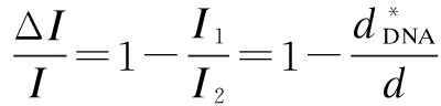
For a typical nanopore with diameter of d and thickness of l, the resistances with (R1) or without (R2) DNA molecule translocation and relative current blockade are written as
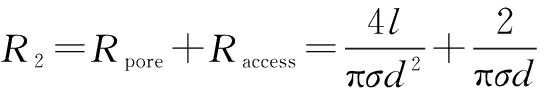
(1)
(2)


(3)
where Rpore is the nanopore resistance; Raccess is the access resistance; dDNA is the diameter of a DNA molecule and ![]() is a parameter relating to the diameter of a DNA molecule (2.2 nm),
is a parameter relating to the diameter of a DNA molecule (2.2 nm), ![]() -1dDNA.
-1dDNA.
For ultrathin nanopore based on Hille’s equation, the resistance without DNA translocation is written as[25]
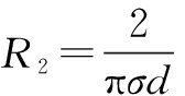
(4)
According to the method described in Ref.[26], when a double stranded DNA molecule is translocating through the nanopore, the resistance model built on a hemisphere schematic can be written as

(5)
Therefore, the relative current blockade ΔI/I for the ultrathin nanopore is written as
(6)
We start the nanopore fabrication on a 100 nm thick low stress silicon nitride (Si3N4) film deposited on a silicon 〈100〉 substrate with the size of 2.5 mm×2.5 mm×0.4 mm by low pressure vapor deposition (LPCVD). On one side, optical lithography and reactive ion etching (RIE) are carried out to produce a 720 μm×720 μm square window up to the silicon nitride layer. Then, anisotropic wet chemical etching of Si is conducted to form a 160 μm×160 μm free-standing Si3N4 membrane. We make a 1 μm blind pore to decrease the nanopore thickness to approximately 10 nm at the center position of the 160 μm×160 μm window area using the focused ion beam (FIB) on the Si3N4 layer. The Si3N4 nanopore is then fabricated by the HR-TEM (FEI Titan 80-300). To obtain a 2D material nanopore, we have to prefabricate a 1 μm through pore at the center position of the 160 μm×160 μm silicon nitride window and then the CVD-grown graphene on copper sheet is transferred to the surface of Si3N4 with a 1 μm pore. The copper sheet is dissolved with FeCl3 solution. Finally, the graphene on silicon nitride substrate is rinsed and dried. The graphene nanopore is then fabricated by the HR-TEM. The chambers on both sides of the nanopore are filled with the ionic solution consisting of 1 mol/L KCl, 10 mmol/L Tris-HCl and 1 mmol/L EDTA (pH 8.0). λ-DNA (48.5 kbp) was purchased from Takara BIO Inc., with an experimental concentration of 3 μg/mL in the electrolyte. The ionic currents of the nanopores with or without DNA translocation are acquired by using a resistive feedback amplifier (HEKA EPC10, HEKA Elektronik) at 200 kHz with low-pass filtering at 10 kHz through Ag/AgCl electrodes. All the current measurements are conducted inside a dark Faraday cage.
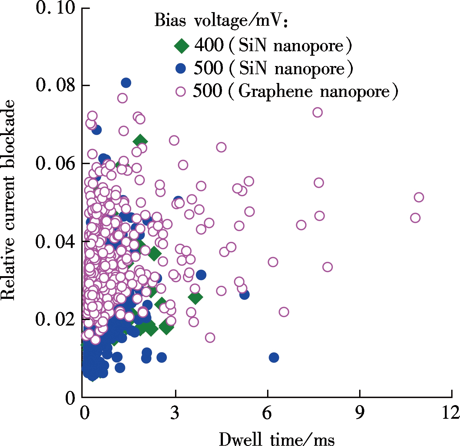
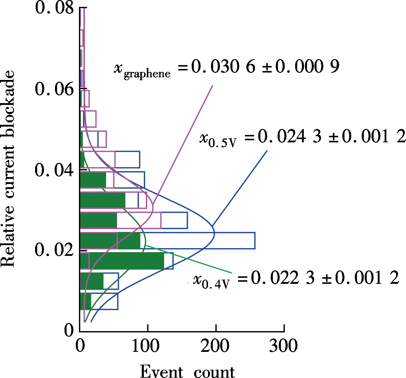
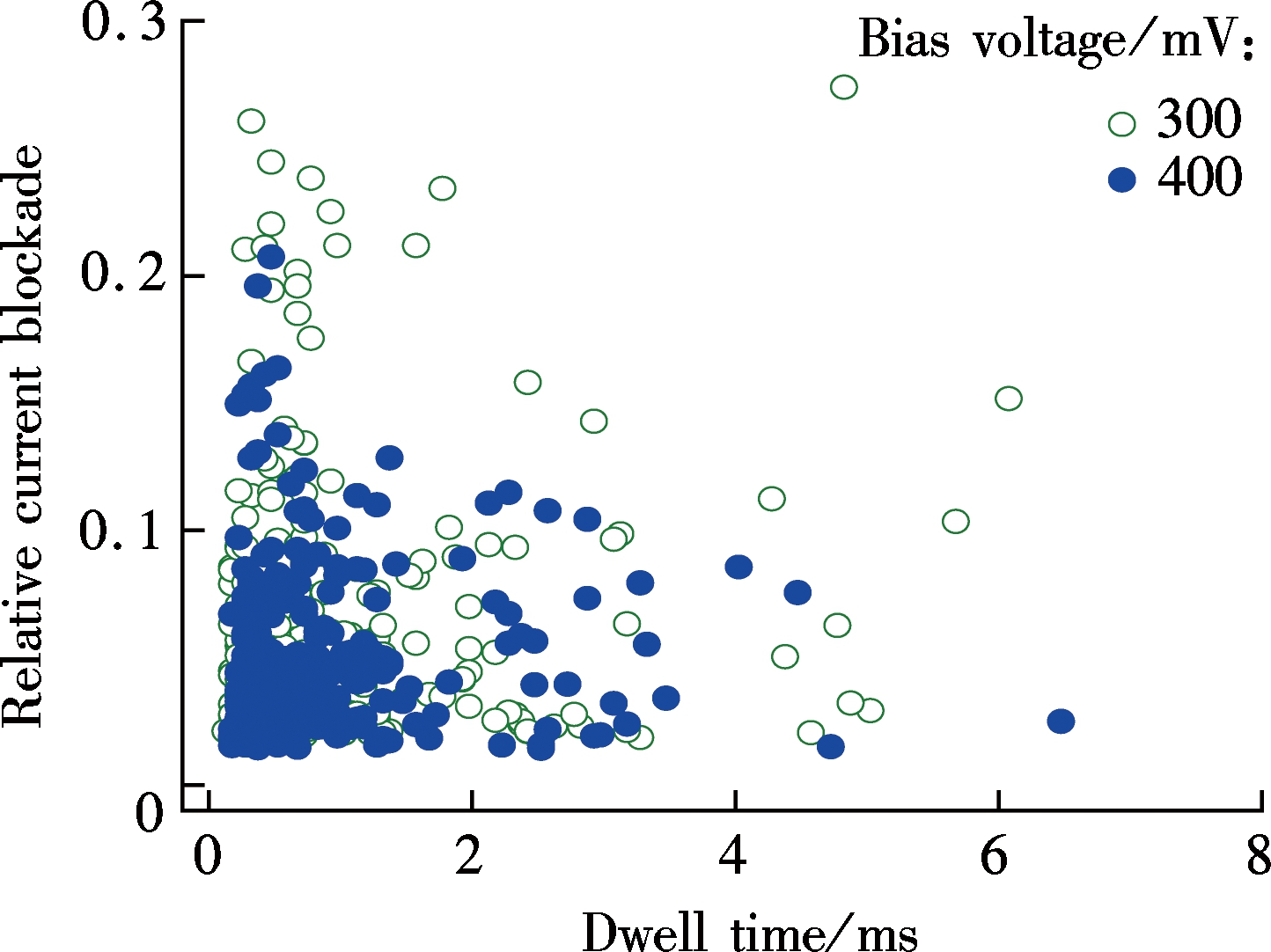
To investigate the effect of nanopore thickness on a relative current blockade, we prepared two kinds of nanopores which are the conventional Si3N4 nanopore and ultrathin graphene nanopore. The diameter of the silicon nitride nanopore is about 12 nm with a thickness of 10 nm. The diameter of graphene nanopore is about 5 nm which is about one to two layers thick. Fig.2(a) shows the scatter plot of the relative current blockade with the dwell time of λ-DNA transport events for these two nanopores. The histogram in Fig.2(b) shows that the Gaussian fitted current peaks for silicon nitride nanopore are x0.5V=0.024 3±0.001 2 and x0.4V=0.022 3±0.001 2 for 500 mV bias voltage and 400 mV bias voltage, respectively, which
(a)
(b)Fig.2 λ-DNA translocation through silicon nitride and graphene nanopores. (a) Scatter plot; (b) Histogram of the relative current blockade vs. the dwell time
are quite close to each other, indicating that the voltage is independent of the relative current blockade. The fitted relative current blockade peak for graphene nanopore is xG=0.030 6±0.000 9, which is only 25.9% higher than that for the Si3N4 nanopore.
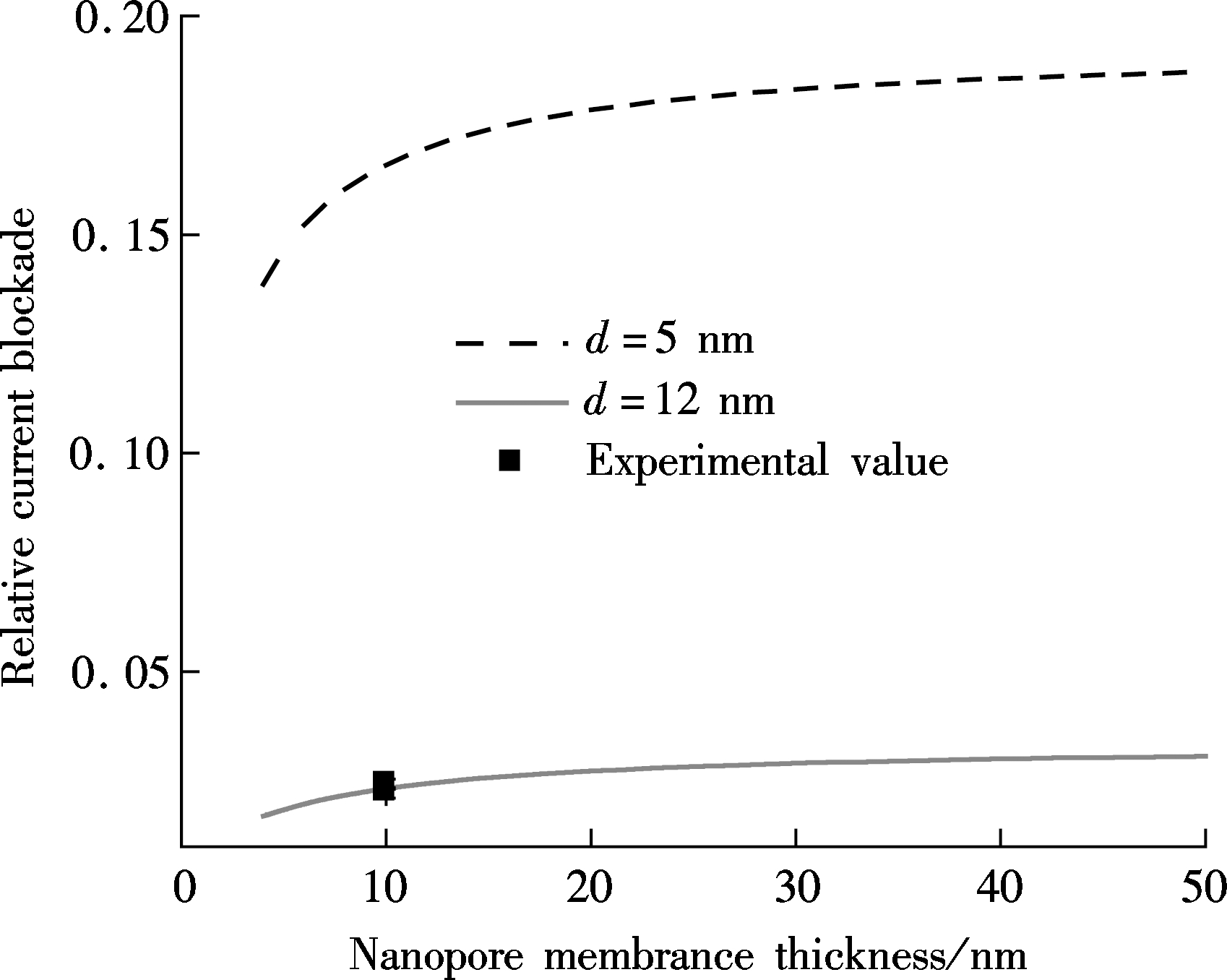
To quantitatively show the thickness dependence, the relative current blockades for these two kinds of nanopores are estimated by Eq.(3) and Eq.(6) and are shown in Fig.3. In Fig.3(a), the relative current blockade is plotted with nanopore thickness ranging from 4 to 50 nm by setting the diameter as 12 nm for the Si3N4 nanopore. It is noted that the relative current blockade gradually decreases as the nanopore thickness decreases, which indicates that the 2D material nanopore cannot effectively promote the spatial resolution for DNA translocation though nanopore. Furthermore, the relative current blockade is increased about fivefold by narrowing the nanopore diameter from 12 to 5 nm. Herein, the relative current blockade for graphene is much smaller than that in the Si3N4 nanopore with a 5 nm diameter, as shown in Fig.3(b). Thus, the diameter reduction is currently the most effective method for enriching the spatial resolution but with a loss on capture rate[26] and a limitation on the closeness to the diameter of the DNA molecule[27-28].
(a)
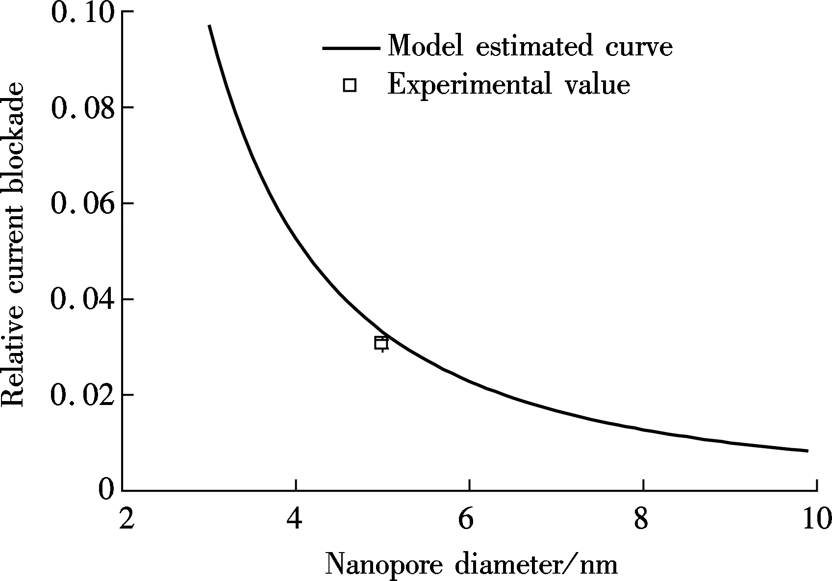
(b)Fig.3 The relative current blockade analysis. (a) Silicon nitride nanopore; (b) Graphene nanopore
The resistance in the access region is gaining more and more attention due to its non-negligible role in the ultrathin nanopore system[24, 29-30]. It is shown that the nanopore resistance is influenced by approaching the AFM tip into the pore mouth region[30]. As shown in Eq.(1), for a long nanopore the access resistance is small compared with the pore resistance which can be ignored when analyzing the biomolecules’ transport behavior. With the wide application of 2D materials showing the superiority of thickness close to the single nucleotide, it is noted that the access resistance becomes more noticeable and even the biomolecules’ approaching or bumping behavior[31] can influence the ionic current, which will multiply the difficulties for signal analysis.
Since the bio-nanopores such as a-hemolysin channel have the structure of β barrel[32-33]and a superior resolution, we mimic the structure of the a-hemolysin nanopore by prefabricating a region to undertake the overall resistance to lower the access resistance, as shown in Fig.4.
(a)
(b)

(c)Fig.4 Two-stage structure for promoting λ-DNA translocation resolution. (a) Scatter plot; (b) Histogram of the relative current blockade vs. the dwell time; (c) Schematic of two-stage nanopore structure
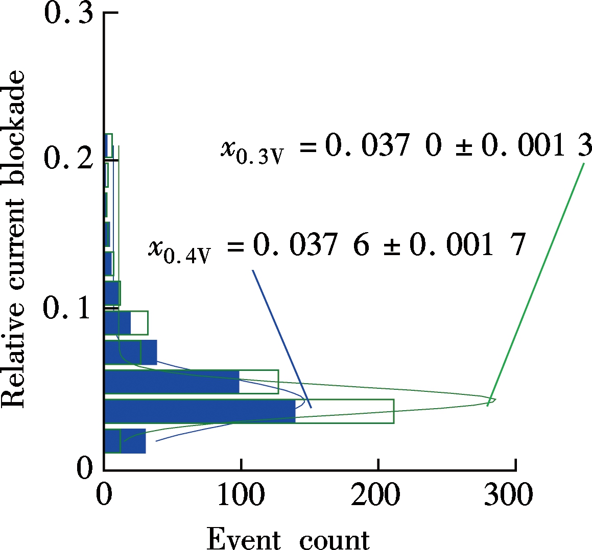
We choose a Si3N4 nanopore area with a diameter of about 30 nm (d0) and a thickness of 20 nm (l0) to assist the 5 nm diameter graphene nanopore to form a two-stage structure. The Gaussian fitted relative current peaks are x0.4V=0.037 6±0.001 7 and x0.3V=0.037 0±0.001 3 for 400 mV and 300 mV biased voltage, respectively. The fitted relative current peak for 400 mV is about 21.9% higher than that without the two-stage structure. However, this method only promotes the overall blockade current to a deeper level which may help overcome the signal noise, and there is still a long way that has to be paved for amplifying the difference among four types of nucleotides.
The spatial resolution of DNA translocation through solid-state nanopore will gain more and more attention before the final realization of the third generation DNA sequencing. We here show the relationship of the DNA translocation through nanopore and access region. It is noted that the relative current blockade can be effectively increased by decreasing the nanopore diameter. However, it is still certain that the relative current blockade decreases as the nanopore thickness decreases. 2D materials do have the advantages for DNA translocation behavior due to their atomic layer thickness. As the nanopore thickness reduces to subnanometer thickness, the access resistance becomes dominant for the overall resistance of the nanopores system. Compared the inner nanopore region, access region has a much broader area, and the narrow DNA molecule can only induce limited ionic current change in this area. To induce the access region resistance into the nanopore area, the two-stage setup by setting the predefined 30 nm diameter Si3N4 area which supports the 5 nm graphene nanopore is designed, which can lead to a 21.9% increase in the relative current blockade. To further enlarge the difference among four single nucleotides, more effort should be made such as creating asymmetrical salt concentrations on both sides of nanopore or increasing the interaction between the nanopore and DNA molecule to promote high spatial resolution.
References:
[1]Venkatesan B M, Bashir R. Nanopore sensors for nucleic acid analysis[J]. Nature Nanotechnology, 2011, 6(10): 615-624. DOI:10.1038/nnano.2011.129.
[2]Branton D, Deamer D W, Marziali A, et al. The potential and challenges of nanopore sequencing[J].Nature biotechnology, 2008, 26(10): 1146-1153. DOI:10.1038/nbt.1495.
[3]Dekker C. Solid-state nanopores[J]. Nature Nanotechnology, 2007, 2(4): 209-215. DOI:10.1038/nnano.2007.27.
[4]van den Hout M, Vilfan I D, Hage S, et al. Direct force measurements on double-stranded RNA in solid-state nanopores[J]. Nano Letters, 2010, 10(2): 701-707. DOI:10.1021/nl903925a.
[5]Nelson E M, Li H, Timp G. Direct, concurrent measurements of the forces and currents affecting DNA in a nanopore with comparable topography[J]. ACS Nano, 2014, 8(6): 5484-5493. DOI:10.1021/nn405331t.
[6]Keyser U F, van der Does J, Dekker C, et al. Optical tweezers for force measurements on DNA in nanopores[J]. Review of Scientific Instruments, 2006, 77(10): 105105. DOI:10.1063/1.2358705.
[7]Smeets R M M, Keyser U F, Dekker N H, et al. Noise in solid-state nanopores[J]. Proceedings of the National Academy of Sciences of the United States of America, 2008, 105(2): 417-421.
[8]Ciccarella P, Carminati M, Ferrari G, et al. Integrated low-noise current amplifier for glass-based nanopore sensing[C]//2014 10th Conference on PhD Research in Microelectronics and Electronics.Grenoble, France, 2014: 1-4. DOI:10.1109/prime.2014.6872701.
[9]Tabard-Cossa V, Trivedi D, Wiggin M, et al. Noise analysis and reduction in solid-state nanopores[J].Nanotechnology, 2007, 18(30): 305505. DOI:10.1088/0957-4484/18/30/305505.
[10]Kumar A, Park K B, Kim H M, et al. Noise and its reduction in graphene based nanopore devices[J].Nanotechnology, 2013, 24(49): 495503. DOI:10.1088/0957-4484/24/49/495503.
[11]Wu G, Zhang Y, Si W, et al. Integrated solid-state nanopore devices for third generation DNA sequencing[J]. Science China—Technological Sciences, 2014, 57(10): 1925-1935. DOI:10.1007/s11431-014-5644-8.
[12]Traversi F, Raillon C, Benameur S M, et al. Detecting the translocation of DNA through a nanopore using graphene nanoribbons[J]. Nature Nanotechnology, 2013, 8(12): 939-945. DOI:10.1038/nnano.2013.240.
[13]Xie P, Xiong Q, Fang Y, et al. Local electrical potential detection of DNA by nanowire-nanopore sensors[J]. Nature Nanotechnology, 2011, 7(2): 119-125. DOI:10.1038/nnano.2011.217.
[14]Ivanov A P, Instuli E, McGilvery C M, et al. DNA tunneling detector embedded in a nanopore[J]. Nanoletters, 2010, 11(1): 279-285. DOI:10.1021/nl103873a.
[15]Fanget A, Traversi F, Khlybov S, et al. Nanopore integrated nanogaps for DNA detection[J]. Nano Lett, 2014, 14(1): 244-249. DOI:10.1021/nl403849g.
[16]King G M, Golovchenko J A. Probing nanotube-nanopore interactions[J]. Physical Review Letters, 2005, 95(21): 216103. DOI:10.1103/PhysRevLett.95.216103.
[17]Heng J B, Aksimentiev A, Ho C, et al. Beyond the gene chip[J]. Bell Labs Technical Journal, 2005, 10(3): 5-22. DOI:10.1002/bltj.20102.
[18]Sigalov G, Comer J, Timp G, et al. Detection of DNA sequences using an alternating electric field in a nanopore capacitor[J]. Nano Letters, 2008, 8(1): 56-63. DOI:10.1021/nl071890k.
[19]Gracheva M E, Xiong A, Aksimentiev A, et al. Simulation of the electric response of DNA translocation through a semiconductor nanopore-capacitor[J]. Nanotechnology, 2006, 17(3): 622-633. DOI:10.1088/0957-4484/17/3/002.
[20]Liu K, Feng J, Kis A, et al. Atomically thin molybdenum disulfide nanopores with high sensitivity for DNA translocation[J]. ACS Nano, 2014, 8(3): 2504-2511. DOI:10.1021/nn406102h.
[21]Liu S, Lu B, Zhao Q, et al. Boron nitride nanopores: Highly sensitive DNA single-molecule detectors[J].Advanced Materials, 2013, 25(33): 4549-4554. DOI:10.1002/adma.201301336.
[22]Venkatesan B M, Dorvel B, Yemenicioglu S, et al. Highly sensitive, mechanically stable nanopore sensors for DNA analysis[J]. Advanced Materials, 2009, 21(27): 2771-2776.
[23]Garaj S, Hubbard W, Reina A, et al. Graphene as a subnanometre trans-electrode membrane[J]. Nature, 2010, 467(7312): 190-193. DOI:10.1038/nature09379.
[24]Kowalczyk S W, Grosberg A Y, Rabin Y, et al. Modeling the conductance and DNA blockade of solid-state nanopores[J]. Nanotechnology, 2011, 22(31): 315101. DOI:10.1088/0957-4484/22/31/315101.
[25]Hille B. Ionic channels in nerve membranes[J]. Progress in Biophysics and Molecular Biology, 1970, 21: 1-32. DOI:10.1016/0079-6107(70)90022-2.
[26]Wanunu M, Morrison W, Rabin Y, et al. Electrostatic focusing of unlabelled DNA into nanoscale pores using a salt gradient[J]. Nature Nanotechnology, 2010, 5(2): 160-165. DOI:10.1038/nnano.2009.379.
[27]Merchant C A, Healy K, Wanunu M, et al. DNA translocation through graphene nanopores[J]. Nano Letters, 2010, 10(8): 2915-2921. DOI: 10.1021/nl101046t.
[28]Schneider G F, Kowalczyk S W, Calado V E, et al. DNA translocation through graphene nanopores[J]. Nano Letters, 2010, 10(8): 3163-3167. DOI:10.1021/nl102069z.
[29]Hall J E. Access resistance of a small circular pore[J]. The Journal of General Physiology, 1975, 66(4): 531-532. DOI:10.1085/jgp.66.4.531.
[30]Hyun C, Rollings R, Li J. Probing access resistance of solid-state nanopores with a scanning-probe microscope tip[J]. Small, 2012, 8(3): 385-392. DOI:10.1002/smll.201290017.
[31]Goepfrich K, Kulkarni C V, Pambos O J, et al. Lipid nanobilayers to host biological nanopores for DNA translocations[J]. Langmuir, 2013, 29(1): 355-364. DOI:10.1021/la3041506.
[32]Kasianowicz J J, Brandin E, Branton D, et al. Characterization of individual polynucleotide molecules using a membrane channel[J]. Proceedings of the National Academy of Sciences, 1996, 93(24): 13770-13773. DOI:10.1073/pnas.93.24.13770.
[33]Clarke J, Wu H C, Jayasinghe L, et al. Continuous base identification for single-molecule nanopore DNA sequencing[J]. Nature Nanotechnology, 2009, 4(4): 265-270. DOI:10.1038/nnano.2009.12.
Citation:Wu Gensheng, Zhang Yin, Si Wei, et al.Current blockade mechanism for DNA translocation through solid-state nanopore with different membrane thickness[J].Journal of Southeast University (English Edition),2016,32(3):301-306.DOI:10.3969/j.issn.1003-7985.2016.03.007.
DOI:10.3969/j.issn.1003-7985.2016.03.007
摘要:通过改变固态纳米孔薄膜厚度,揭示了λ-DNA在电场作用下通过纳米孔时堵塞离子电流的作用机理.纳米孔的电导主要由孔内电阻和孔口电阻构成,当纳米孔长度逐渐减小到与原子层厚度相等时,电导主要由孔口电阻主导.根据已有的纳米孔孔口电阻模型,推导出一个简化的DNA分子堵塞纳米孔的相对离子电流模型,定量地描述了纳米孔薄膜厚度与相对堵塞电流大小之间的关系.结果表明, 相对堵塞电流随着纳米孔直径的减小而增加,但随着纳米孔厚度的减小而减小.为提高相对堵塞电流,提出了一种二级结构,该结构设置了一个更小的纳米孔孔口电阻区域.实验结果显示,该结构使相对堵塞电流提高了21.9%.
关键词:纳米孔;基因测序;相对堵塞电流;薄膜厚度
中图分类号:O561.4
Received:2016-02-16.
Foundation item:s:The Natural Science Foundation of Jiangsu Province (No.BK20160935), the Natural Science Foundation of Higher Education Institutions of Jiangsu Province (No.16KJB460015).
Biography:Wu Gensheng(1986—),male,doctor,lecturer, genshengwu@126.com.