(a)
Abstract:A novel programmable gain amplifier (PGA) based on a signal-summing topology is proposed. Different from conventional signal-summing variable gain amplifiers (VGA), a binary-weighted switching technique is employed to vary the current-steering transistors’ aspect ratio to change their transconductance, and hence, an accurate gain step size of 6 dB is achieved. The constant-gm biasing technique and the matching of the transistors and resistors ensures that the gain of the proposed topology is independent of the variation of process, voltage and temperature (PVT). P-well NMOS (N-metal oxide semiconductor)transistors are utilized to eliminate the influence of back-gate effect which will induce gain error. The source-degeneration technique ensures good linearity performance at a low gain. The proposed PGA is fabricated in a 0.18 μm CMOS (complementary metal oxide semiconductor) process. The measurement results show a variable gain ranging from 0 to 24 dB with a step size of 6 dB and a maximum gain error of 0.3 dB . A constant 3 dB bandwidth of 210 MHz is achieved at different gain settings. The measured output 3rd intercept point (OIP3) and minimum noise figure (NF) are 20.9 dBm and 11.1 dB, respectively. The whole PGA has a compact layout of 0.068 mm2. The total power consumption is 4.8 mW under a 1.8 V supply voltage.
Key words:programmable gain amplifier; variable gain amplifier; signal-summing topology; constant-gm
The automatic gain control (AGC) circuit is an important building block which can be found in many applications, such as the disk driver, wireless communication, etc[1-4]. Due to the indeterminate transmitted power and the variable distance between devices, the received signal level varies over a wide range. Therefore, AGC is necessary to automatically adjust the gain of the receiver so as to provide a relatively constant amplitude signal to the analog-to-digital converter (ADC), which helps to meet its dynamic range requirement[5]. In an AGC, a VGA is the key component. There are two main stream VGAs, a continuous gain control VGA and a discrete or digital gain control VGA, which is also called a PGA. The PGA has become more popular in many applications due to its more convenient and accurate gain control. The programmable gain can be obtained by switching on the transconductance, load resistance, or the resistance ratio[6].
In order to maintain a constant settling time for the AGC, the VGA gain should have a dB-linear characteristic.[7]. Several dB-linear gain VGAs have been designed in a bipolar process, because the bipolar transistor has the inherent exponential-law characteristic of the collector current IC and the base-emitter voltage VBE, which can be expressed as IC = IS exp(VBE/ VT ), where IS and VT denote the reverse saturation current and the thermal voltage, respectively[8]. However, the bipolar VGA typically results in higher power consumption and is not compatible with the CMOS technology. Therefore, a CMOS VGA based on a pseudo exponential function has been developed.
Since the data rates of modern wireless communication standards are increasing significantly, the VGA in the intermediate frequency (IF) amplifying stage requires a broader bandwidth. Even in low data rate applications, such as digital radios and Bluetooth,a large bandwidth VGA is also necessary. In a dual-conversion receiver, to alleviate the image rejection requirement and the complexity of the frequency synthesizer, the first IF is usually set at a high frequency. Therefore, a wideband VGA with coarse gain control after the first mixer is essential. This paper focuses on the design of wideband PGA with coarse gain step size. The fine gain control is achieved by the subsequent gain stages.
1.1 Classical CMOS VGA and PGA techniques
Fig.1(a) shows a conventional signal-summing VGA which has the advantage of broad bandwidth and low noise[9]. The variable gain is obtained by changing the control voltage VC, which steers the signal current coming from the input transistors towards the load resistor. Since the load resistor is constant, the bandwidth will not be influenced by the gain setting. The dominant noise source is the thermal noise and flicker noise of the input transistors, M1 and M2. However, despite these advantages, it is difficult to realize exponential gain control due to the inherent square-law characteristic of MOS transistors. Although a MOS transistor operating in the subthreshold region has an exponential characteristic, it is not preferred due to a decreased linearity, an increased noise and a small gain range. Therefore, an extra circuit for pseudo exponential control voltage is required. The most frequently used pseudo exponential function can be expressed as
(a)
(b)
Fig.1 Conventional topologies of VGAs. (a) Signal-summing VGA;(b) Resistive feedback PGA
e2ax≅![]()
(1)
where a and k are constants. However, the gain range for these approximation functions is less than 20 dB, and the gain linearity error is also significant. Another problem of a signal-summing VGA is that the gain is heavily affected by temperature and process variation. Therefore, the signal summing VGA topology is not preferred in modern receivers.
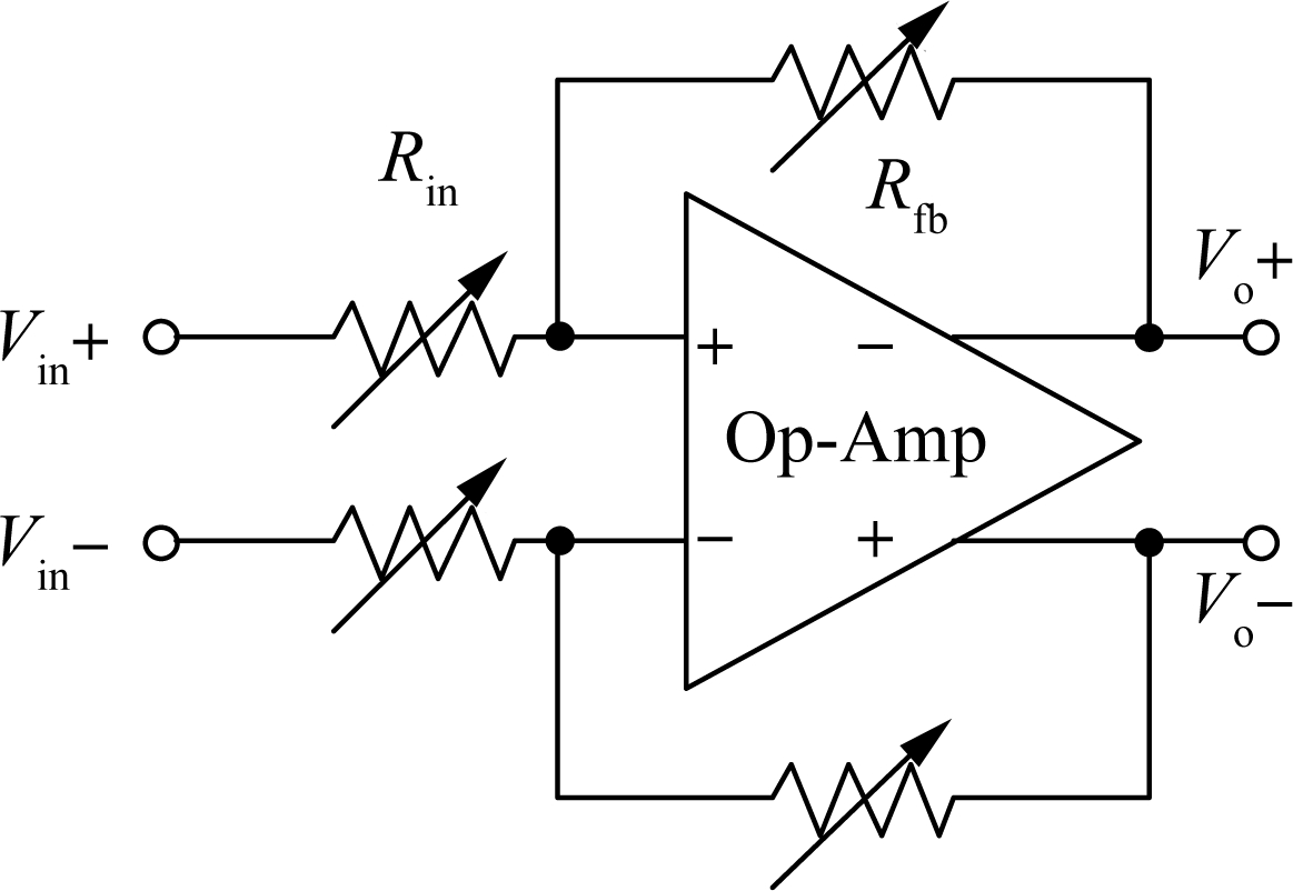
Although the PGA cannot provide continuous gain control, the gain is more accurate than that of the VGA. Fig.1(b) shows a conventional resistive feedback PGA, which has good gain accuracy and linearity. The main disadvantage of this topology is that the bandwidth decreases as the gain increases due to the finite gain bandwidth product (GBW) of the operational amplifier (Op-Amp).Therefore, it is not preferred for high data rates or high IF applications. Since the input resistor increases the input-referred noise directly, more power will be consumed to reduce the noise of the Op-Amp and to drive the smaller resistor to achieve an acceptable noise performance.
As shown in this paragraph, the conventional VGA as well as PGA suffer from a tradeoff among a constant bandwidth, a good noise performance, and accurate, temperature- and process-independent gain.
1.2 Signal-summing PGA
In order to obtain constant bandwidth and good noise performance, a signal-summing topology is the most preferred. In a signal-summing VGA shown in Fig.1(a), the gain can be expressed as
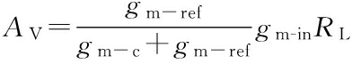
(2)
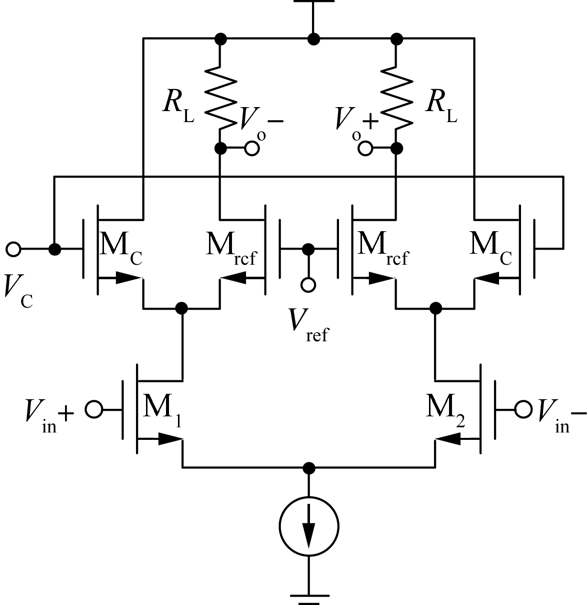
Usually, the CG transistors MC and Mref have the same aspect ratio. The signal-summing VGA employs VC to change the bias current distribution of MC and Mref to change their transconductance. However, the transconductance of a MOS transistor depends on not only the bias current, but also the aspect ratio. Therefore, a signal-summing VGA can also be achieved by changing the aspect ratio of MC and Mref. Fig.2 shows the schematic of a digitally controlled signal-summing VGA employing a binary-weighted switching technique. The effective aspect ratio of MC and Mref are ![]() and
and ![]() , respectively. The total aspect ratio is constant and is given as 8 W/L. The programmable gain can then be expressed as
, respectively. The total aspect ratio is constant and is given as 8 W/L. The programmable gain can then be expressed as
(3)
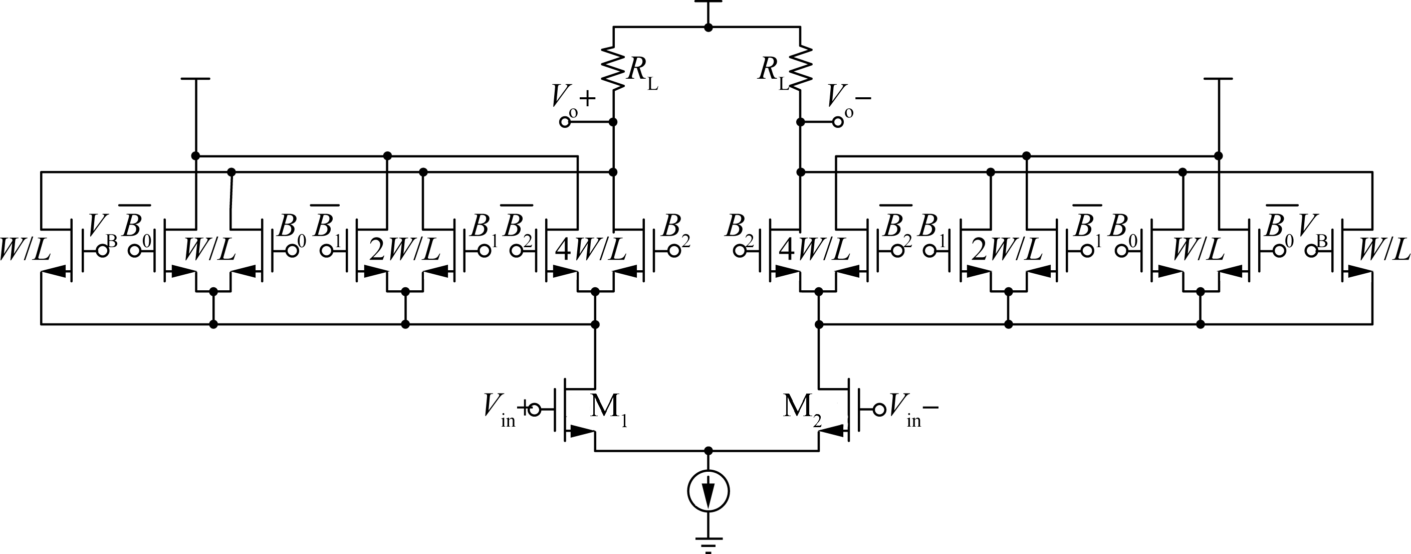
Fig.2 The digitally controlled signal-summing VGA
To obtain a 6 dB step size, only four control codes will be employed, and they are (B0B1B2)=000, 100, 110, 111.
This topology has three stacked transistors and a load resistor, and hence the output swing is limited, deteriorating the linearity performance. Therefore, the bias voltage of the input transistors and the switching transistors should be designed carefully. The voltage representing control bit 1 biases the switching stage, and its minimum value is
VB=Vthn+3Vovn
(4)
where Vthn and Vovn are the threshold voltage and overdrive voltage of the NMOS, respectively. In general, the value of the threshold voltage in the 180 nm CMOS process is 450 mV. Assuming that the overdrive voltage is 200 mV, VDD,min is 1.05 V. In this work, the back-gate effect is taken into consideration, and a 1.2-V VB is adopted. Since a high output impedance voltage supply is not suitable for the digital control circuits, a 1.2-V low dropout (LDO) regulator depicted in Fig.3 is designed.
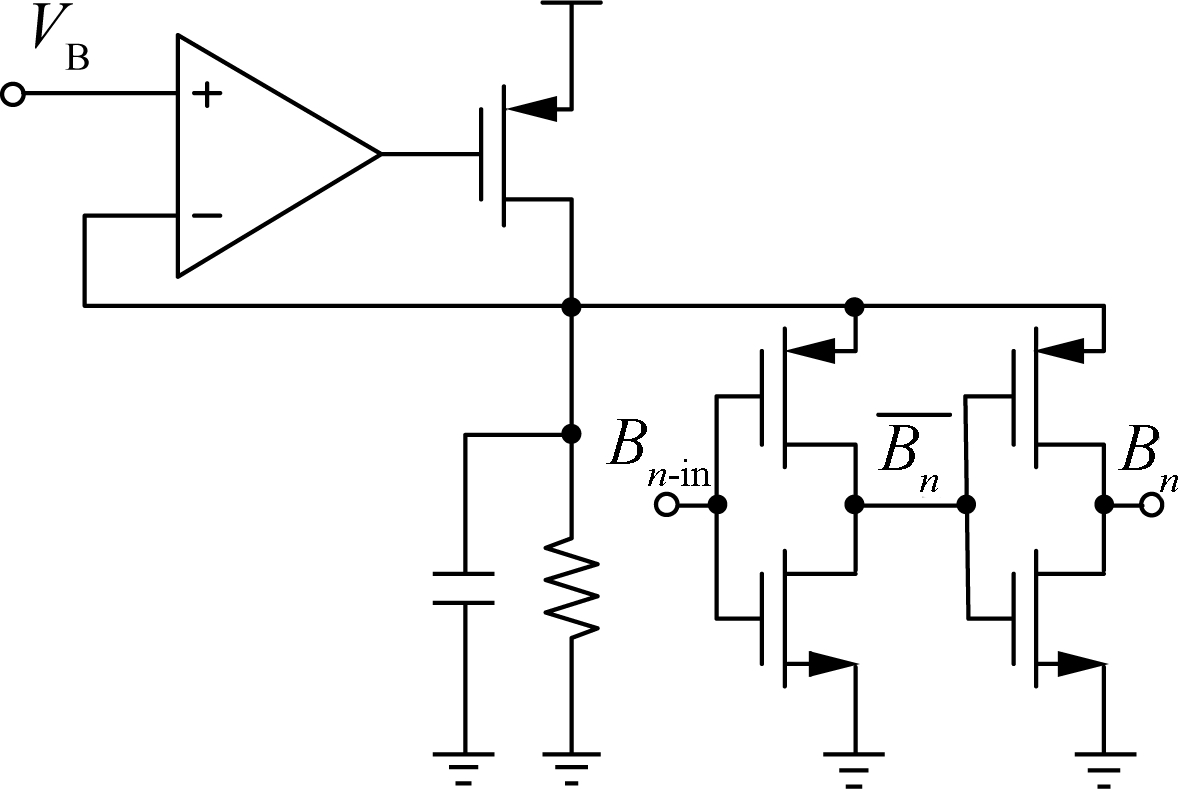
Fig.3 LDO for digital circuits
1.3 Constant-gm bias
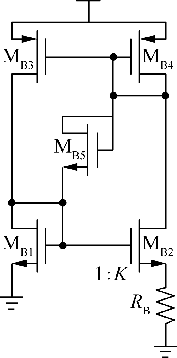
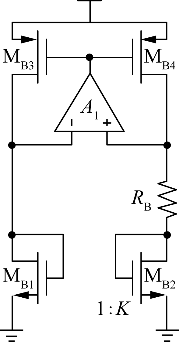
Even though the topology shown in Fig.2 has an accurate gain step size of 6 dB, the initial gain value is unpredictable due to the process, voltage and temperature (PVT)-dependent gm-in and RL. From Eq.(4), there are two methods to achieve accurate gain: The first is to achieve constant gm-in and RL by employing additional techniques, and the second is to obtain constant product of gm-in and RL. A constant-gm biasing technique has been employed in maintaining gain, bandwidth and noise stable[10-11]. The typical constant-gm circuit is depicted in Fig.4(a). To eliminate the influence of the back-gate effect and channel-length modulation, an improved topology utilizing an Op-Amp A1 is shown in Fig.4(b). The transconductance of MB1 can be expressed as
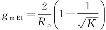
(5)
From Eq.(5), the transconductance only depends on the bias resistor RB and the geometries of transistors MB1 and MB2. However, the sheet resistance of on-chip resistors also depends on temperature. The ratio of the maximum value of sheet resistance to the minimum value often exceeds 150% over the operating temperature range of -25 to 125 ℃. Thus, this approach cannot provide a true constant gm , and in practice, a precise off-chip resistor is used. If off-chip RB is adopted to achieve accurate gain, the load resistor RL should also be off-chip. Off-chip components decrease the chip integration level and are not suitable for modern receivers[12-13].
(a)
(b)
Fig.4 Constant-gm bias circuits. (a) Classical constant-gm bias; (b) More accurate constant-gm bias
Eq.(5) prompts us that if the load resistor and the bias resistor are matched and have the same temperature coefficient, a PVT-independent gain will be obtained, and it can be expressed as
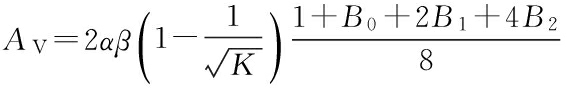
(6)
where α is the transconductance ratio of M1,2 in Fig.2 and MB1in Fig.4; β is the resistance ratio of RL and RB. The gain is only determined by the ratios and control code. However, if the back-gate effect of M1,2is taken into account, the gain will be inaccurate. To fix this problem, P-well technique is employed in this design, and M1,2, MB1,B2 are all P-well NMOS.
1.4 Proposed signal-summing PGA
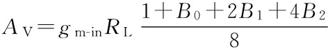
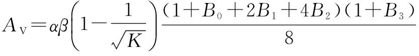
Fig.5 shows the schematic of the proposed signal-summing PGA. The limited linearity is the most significant disadvantage of a signal-summing VGA. The nonlinear distortion has two sources. The first is the transconductance stage’s poor linearity. Without feedback techniques, the nonlinear characteristic of M1,2 is invariant with different gain settings. The second is the limited output swing. When the input signal level is high and the gain is low, the voltage drop across RL is also decreased. Therefore, higher nonlinear distortions will appear at low gains. Source-degeneration technique is effective to improve the linearity of the input transistor. As shown in Fig.5, source-degeneration resistor RSD is employed with a parallel switching transistor M5. The resistor type of RSD is the same as RL and RB, which will ensure that the gain PVT is independent. At the highest gain, the linearity requirement is low and better noise performance is required, and therefore, RSD is shortened by M5 in this case. Since the gain step size is 6 dB, the value of RSD must be 1/gm1. The PMOS M3, M4 and RL are used as a common-mode feedback circuit. This topology ensures that even at the lowest gain, the upper output swing will be at least equal to the threshold voltage of a PMOS. Hence, the linearity of the proposed PGA has been improved by these two techniques. The gain of the proposed PGA is
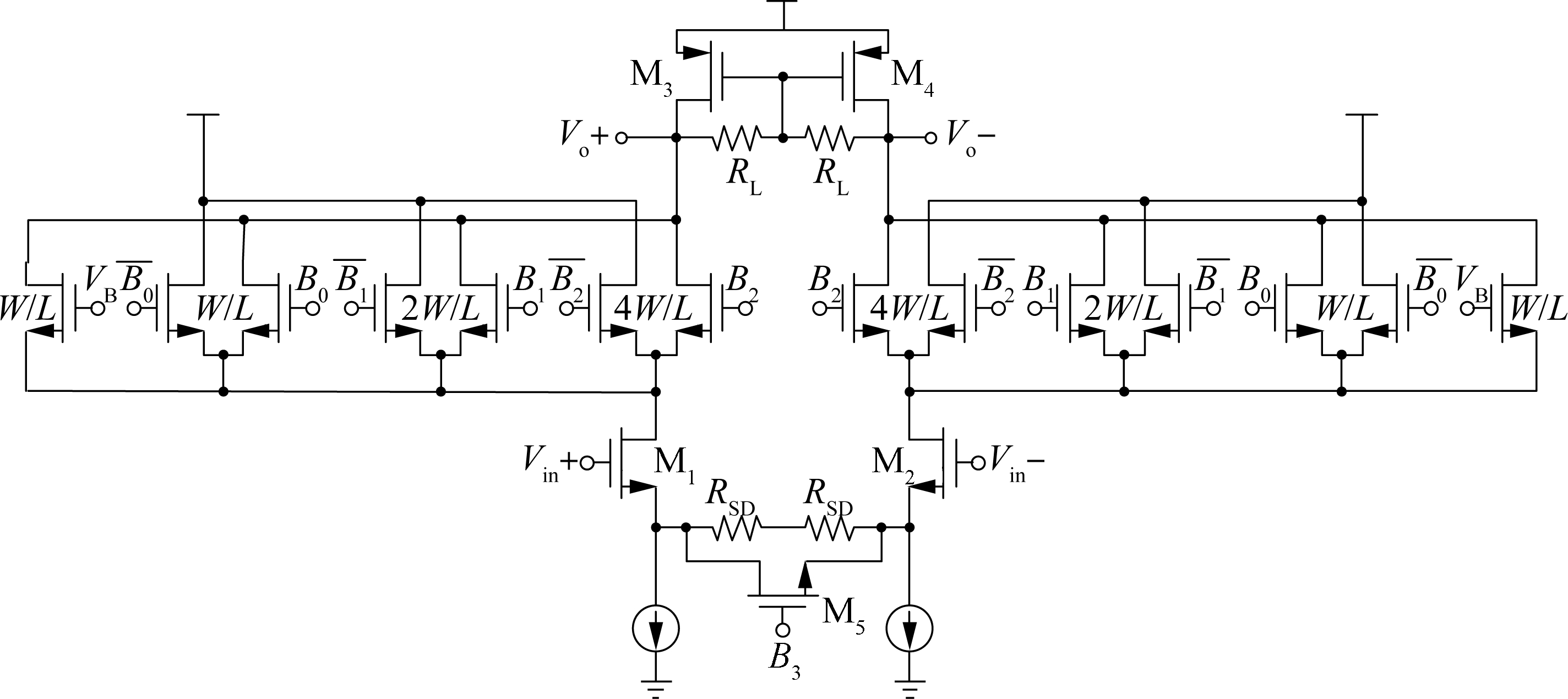
Fig.5 The proposed signal-summing PGA
(7)
where α, β, K are 8, 2 and 4, respectively. Tab.1 gives the control code of different gains. A wideband two-stage Op-Amp in unity gain feedback configuration is also designed as a buffer for measurement. Since the 50 Ω load impedance is low enough, there is no need to employ Miller compensation, and therefore the bandwidth of the Op-Amp is adequate for PGA’s bandwidth measurement.
Tab.1 The gain control code
Gain/dB06121824B3B2B1B000000001001101111111
The PGA was fabricated in a 0.18 μm RF CMOS process. A micrograph of the PGA is shown in Fig.6.
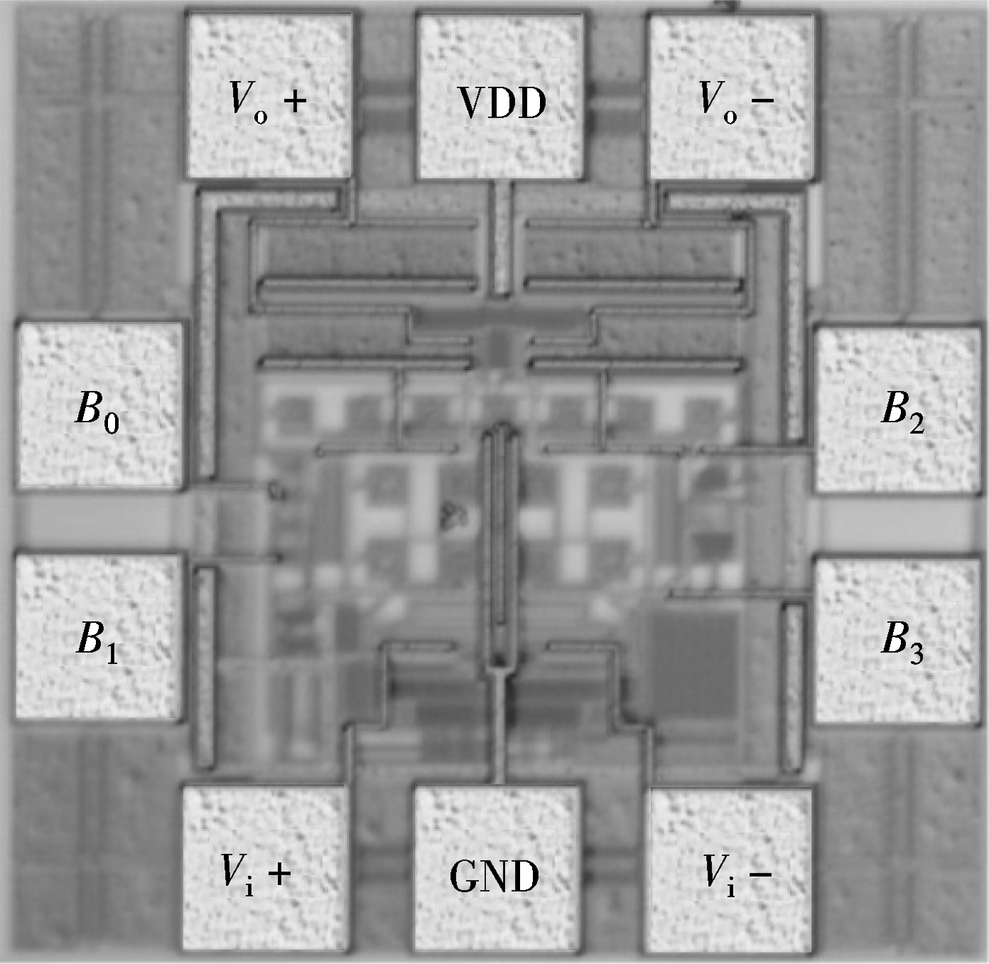
Fig.6 Chip micrograph of PGA
The die area of the core circuit is 0.25 mm×0.27 mm. Two signal-ground-signal (SGS) probes and two 2-pin DC probes were used during the on-wafer measurements. The power consumption of the PGA core circuit is 4.8 mW under a 1.8 V voltage supply.
Fig.7 shows the measured frequency response at different gains. The 3-dB bandwidth remains almost constant, i.e. around 210 MHz. Fig.8 shows the gain and gain error at 10 MHz, and the maximum gain error is -0.3 dB at the maximum gain of 24 dB. Hence, the proposed PGA offers accurately controlled gain. The IP3 measurement result is shown in Fig.9, where 10.2 and 20.9 dBm OIP3 are achieved at 0 and 24 dB, respectively. The source-degeneration resistor improves the third-order nonlinearity effectively. The measured IP1dB is shown in Fig.10, and it can be seen that the IP1dB at 24 dB gain is poor, because not only the source-degeneration resistor is shortened, but also the output amplitude is limited. Fig.11 shows the measured NF at different gains, and the minimum. The die area of the core circuit is 0.25 mm×0.27 mm. Two signal-ground-signal (SGS) probes and two 2-pin DC probes were used during the on-wafer measurements. The power consumption of the PGA core circuit is 4.8 mW under a 1.8 V voltage supply. NF is achieved at 11.1 dB. The performance summary and comparison with other works are listed in Tab.2.
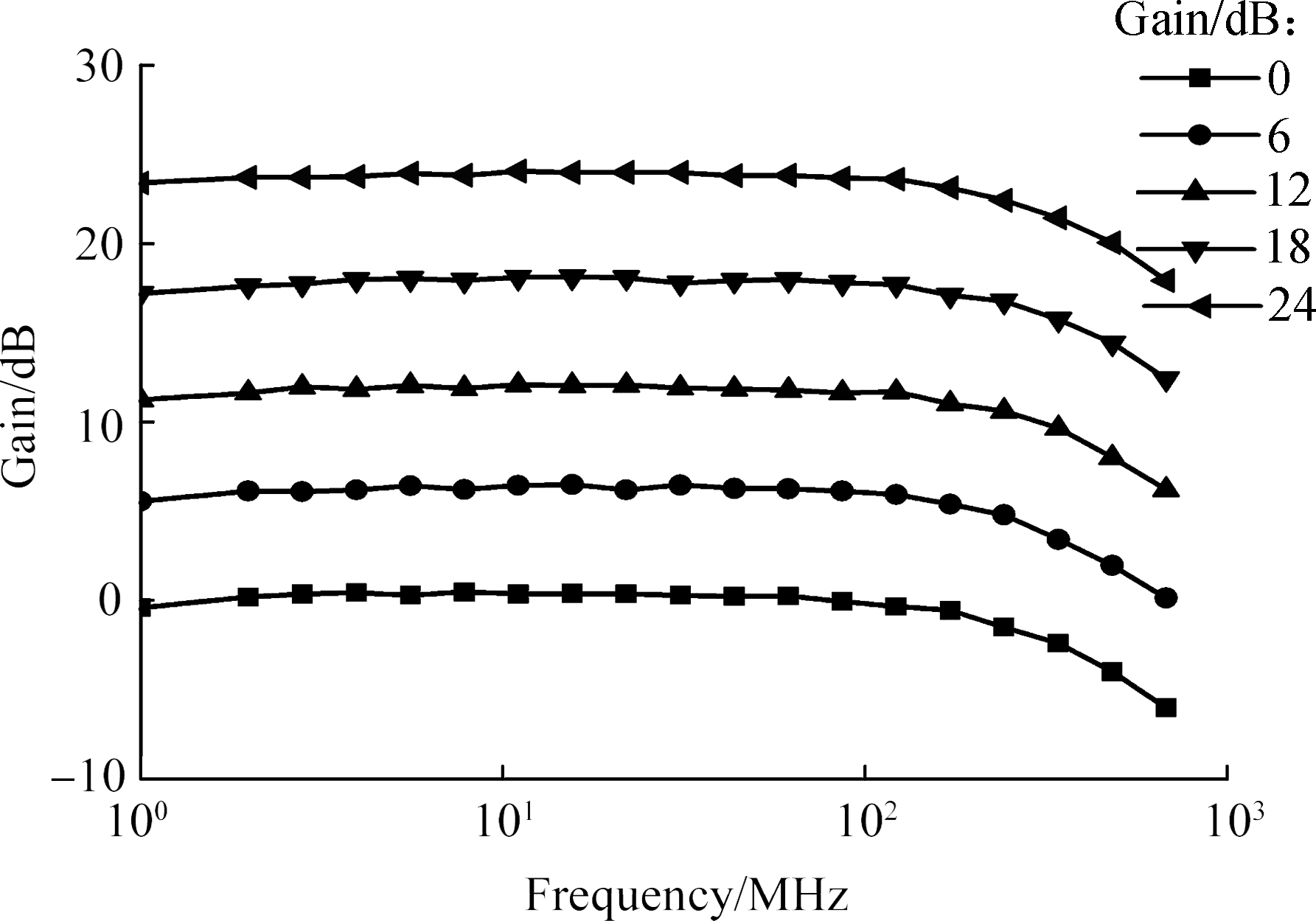
Fig.7 Measured frequency response at different gains
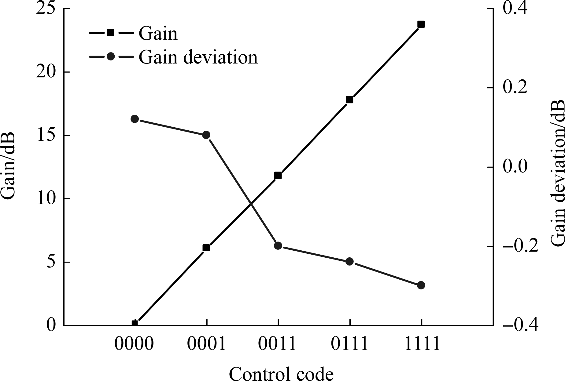
Fig.8 Measured gain and gain error at 10 MHz
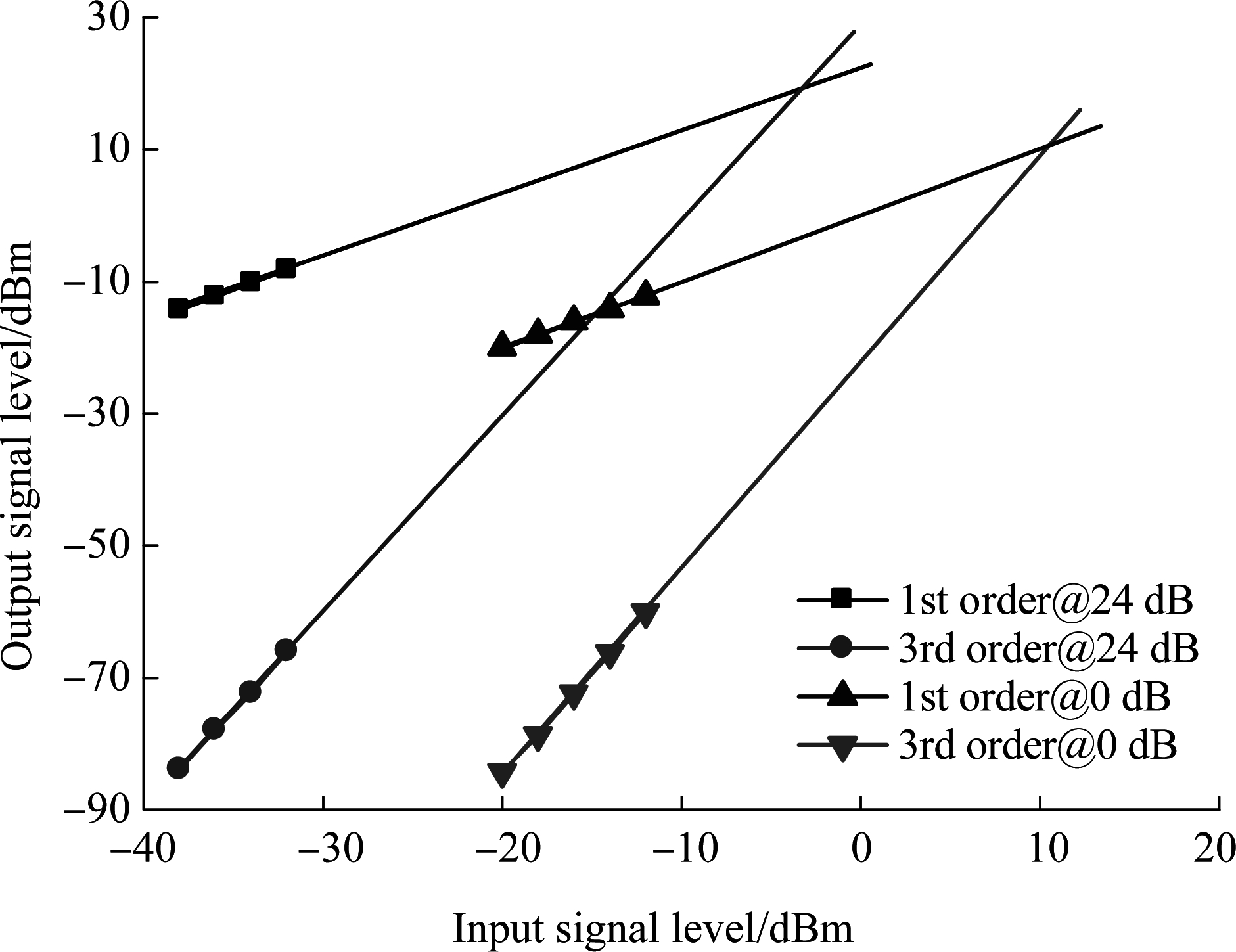
Fig.9 Measured IP3 at minimum and maximum gain
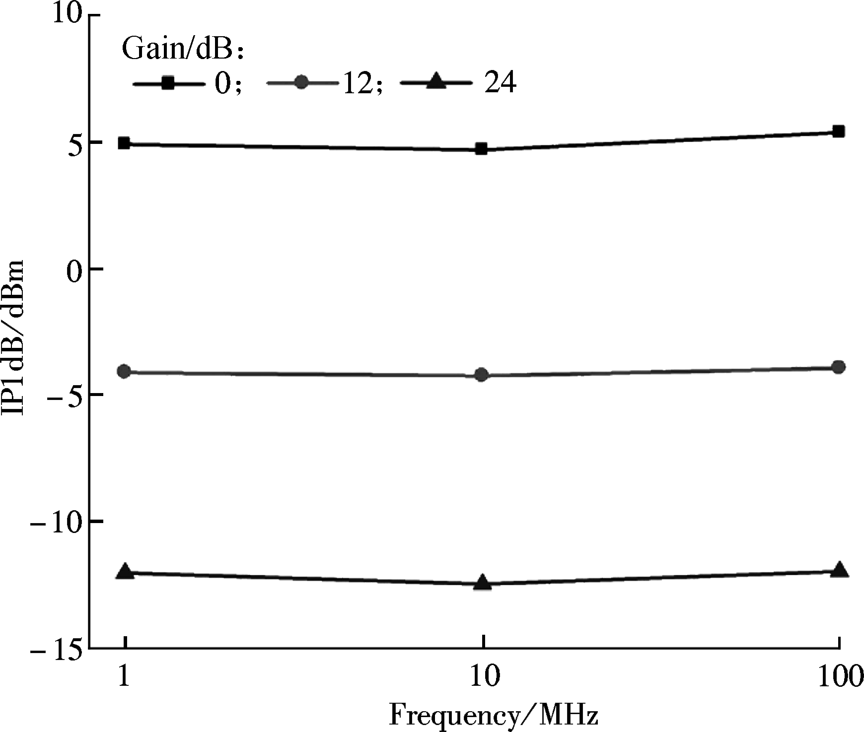
Fig.10 Measured IP1dB vs. frequency at different gains
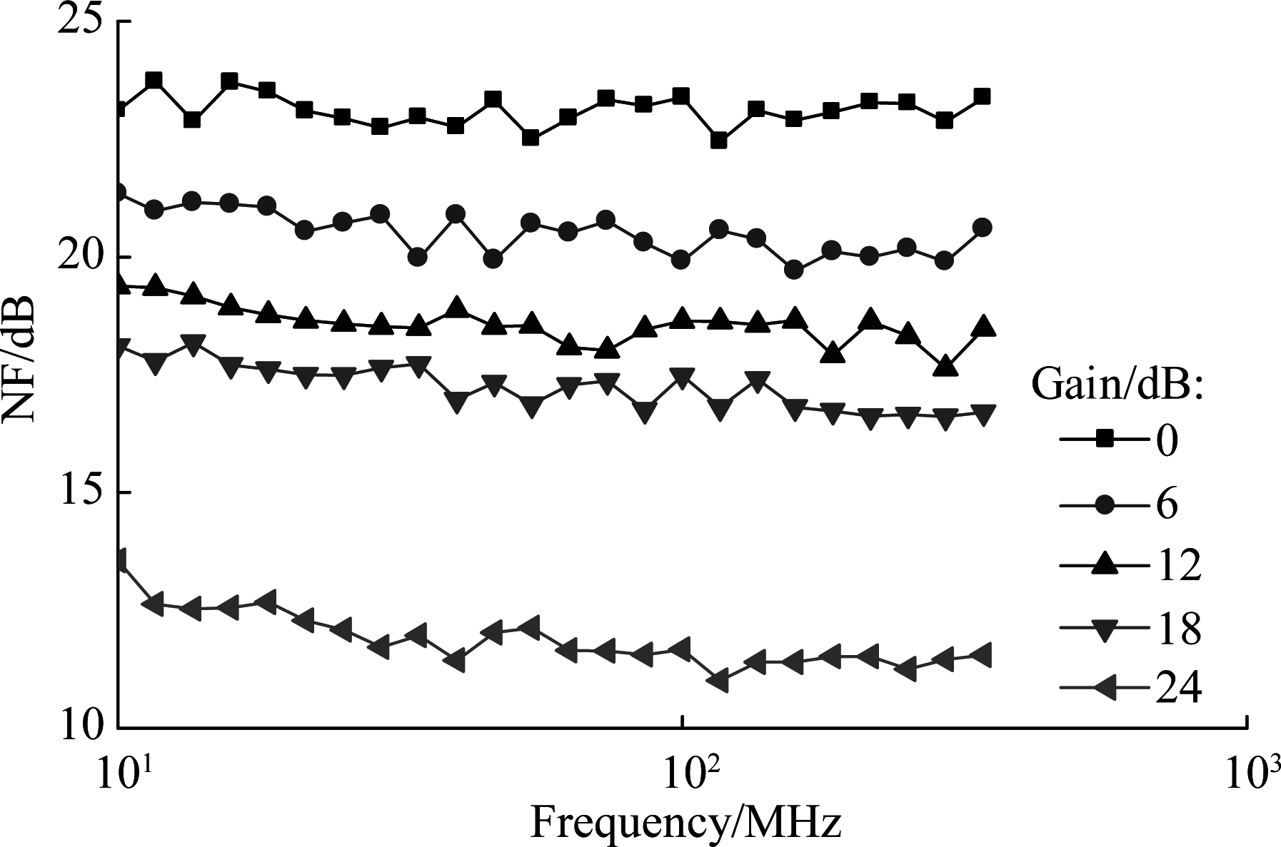
Fig.11 Measured NF at different gains
Tab.2 Performance summary and comparison
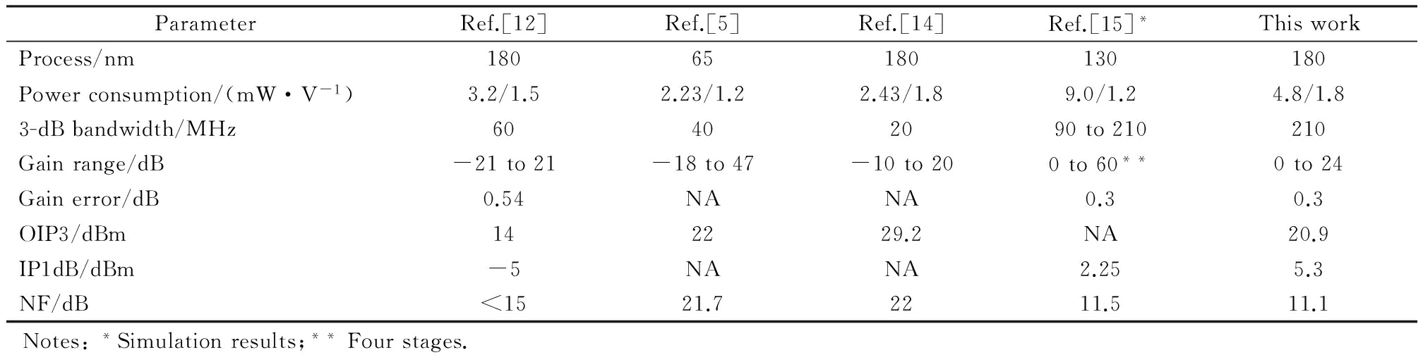
ParameterRef.[12]Ref.[5]Ref.[14]Ref.[15]*ThisworkProcess/nm18065180130180Powerconsumption/(mW·V-1)3.2/1.52.23/1.22.43/1.89.0/1.24.8/1.83-dBbandwidth/MHz60402090to210210Gainrange/dB-21to21-18to47-10to200to60**0to24Gainerror/dB0.54NANA0.30.3OIP3/dBm142229.2NA20.9IP1dB/dBm-5NANA2.255.3NF/dB<1521.72211.511.1Notes:*Simulationresults;**Fourstages.
This paper proposes a novel PGA based on the signal-summing topology. The current-steering stage’s aspect ratio is binary-weighted controlled, and hence, a 6 dB step size is achieved. Constant-gm biasing technique P-well transistors help improve the gain accuracy, and they make the gain PVT-independent. Moreover, the source-degeneration technique ensures good linearity performance at low gains when there is a large input signal. The measurement results show a gain range of 0 to 24 dB with a 6 dB step size and a 0.3 dB gain error. The measured 3-dB bandwidth remains constant at different gains. The measured OIP3 and minimum noise figure are 20.9 dBm and 11.1 dB, respectively. The total power consumption is 4.8 mW under a 1.8 V supply voltage.
[1]Chen J, Shi B. Circuit design of an on-chip temperature-compensated constant transconductance reference [J]. Analog Integrated Circuits and Signal Processing, 2003, 37(3):215-222.DOI: 10.1023/A:1026221809719.
[2]Chen Z, Zheng Y, Choong F C, et al. A low-power variable-gain amplifier with improved linearity: Analysis and design [J]. IEEE Transactions on Circuits and Systems Ⅰ:Regular Papers, 2012, 59(10):2176-2185.DOI:10.1109/tcsi.2012.2185331.
[3]Chu C, Wang Y. A PVT-independent constant-Gm bias technique based on analog computation[J]. IEEE Transactions on Circuits and Systems Ⅱ: Express Briefs,2014,61(10):768-772. DOI:10.1109/tcsii.2014.2345296.
[4]Duong QH, Le Q, Kim CW, et al. A 95 dB linear low-power variable gain amplifier [J]. IEEE Transactions on Circuits and Systems Ⅰ: Regular Papers, 2006,53(8):1648-1657.DOI: 10.1109/TCSI.2006.879058.
[5]Elwan H, Tekin A, Pedrotti K. A differential-ramp based 65 dB-linear VGA technique in 65 nm CMOS [J]. IEEE Journal of Solid-State Circuits, 2009,44(9):2503-2514.DOI:10.1109/jssc.2009.2021446.
[6]Han X, Yuan H M, Pang X M. Design and implementation of an improved constant-Gm bias circuit [C]//8th IEEE Conference on Industrial Electronics and Applications. Melbourne, Australia, 2013:839-842.
[7]Hsu C C, Wu J T. A highly linear 125 MHz CMOS switched-resistor programmable-gain amplifier [J]. IEEE Journal of Solid-State Circuits, 2003, 38(10):1663-1670. DOI:10.1109/jssc.2003.817665.
[8]Lee H D, Lee K A, Hong S. A wideband CMOS variable gain amplifier with an exponential gain control [J]. IEEE Transactions on Microwave Theory & Techniques, 2007, 55(6):1363-1373. DOI:10.1109/tmtt.2007.896787.
[9]Kang S Y, Jang J, Oh I Y,et al. A 2.16 mW low power digitally-controlled variable gain amplifier [J]. IEEE Microwave and Wireless Components Letters, 2010, 20(3):172-174. DOI:10.1109/lmwc.2010.2040222.
[10]Khoury J M. On the design of constant settling time AGC circuits [J]. IEEE Transactions on Circuits and Systems Ⅱ: Analog and Digital Signal Processing, 1998, 45(3):283-294. DOI:10.1109/82.664234.
[11]Lerstaveesin S, Gupta M, Kang D, et al. A 48-860 MHz CMOS low-IF direct-conversion DTV tuner [J]. IEEE Journal of Solid-State Circuits, 2008, 43(9):2013-2024.DOI:10.1109/JSSC.2008.2001900.
[12]Nguyen H H, Lee J S, Lee S G. A binary-weighted switching and reconfiguration-based programmable gain amplifier [J]. IEEE Transactions on Circuits and Systems Ⅱ: Express Briefs, 2009, 56(9):699-703.DOI:10.1109/TCSII.2009.2027958.
[13]Talebbeydokhti N, Hanumolu P K, Kurahashi P, et al. Constant transconductance bias circuit with an on-chip resistor [C]//IEEE International Symposium on Circuits and Systems. Island of Kos, Greece, 2006:2857-2860.
[14]Tsou S C, Li C F, Huang P C. A low-power CMOS linear-in-decibel variable gain amplifier with programmable bandwidth and stable group delay [J]. IEEE Transactions on Circuits and Systems Ⅱ:Express Briefs, 2006, 53(12):1436-1440. DOI:10.1109/tcsii.2006.885399.
[15]Zhang X, Mirabbasi S, Lampe L. A temperature-stable 60 dB programmable-gain amplifier in 0.13 μm CMOS[C]//IEEE International Symposium on Circuits and Systems. Rio de Janeiro, Brazil,2011:1009-1012.
References:
摘要:提出了一种基于信号求和结构的新型可编程增益放大器.不同于传统的信号求和可变增益放大器,在本设计中,通过二进制开关的控制接入分流管的宽长比来实现分流管的跨导改变.二进制的设计可以实现精确的6 dB增益步长.恒跨导偏置技术保证了电路实现精确的增益,且不受工艺、电压和温度变化的影响.P-well NMOS技术消除了背栅效应对增益误差的影响.低增益采用源极退化技术实现,实现了信号强度较大时,电路具有高线性度.所设计的可编程增益放大器采用0.18 μm CMOS工艺制造.测试结果显示,增益范围为0~24 dB,增益步长6 dB,最大增益误差为0.3 dB.在不同增益下,电路都能保证恒定210 MHz带宽.OIP3和最小噪声系数分别为20.9 dBm和11.1 dB.电路版图紧凑,核心面积为0.068 mm2.在1.8 V的电源电压下,消耗4.8 mW功率.
关键词:可编程增益放大器;可变增益放大器;信号求和结构;恒跨导偏置
中图分类号:TN43
Received:2016-11-06.
Foundation item:The National Natural Science Foundation of China (No.61306069).
Citation::Ma Li, Wang Zhigong, Xu Jian. A signal-summing programmable gain amplifier employing binary-weighted switching and constant-gmbias[J].Journal of Southeast University (English Edition),2017,33(2):134-139.
DOI:10.3969/j.issn.1003-7985.2017.02.002.
DOI:10.3969/j.issn.1003-7985.2017.02.002
Biographies:Ma Li (1989—), male, doctor; Wang Zhigong (corresponding author), male, doctor, professor, zgwang@seu.edu.cn.