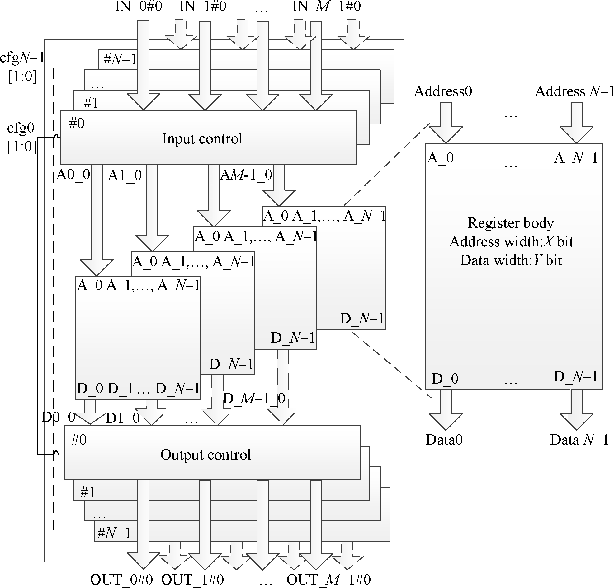
Fig.1 Schematic structure view of cross-domain register file
Abstract:Due to the fact that the register files seriously affect the performance and area of coarse-grained reconfigurable cryptographic processors, an efficient structure of the distributed cross-domain register file is proposed to realize a cryptographic processor with a high performance and a low area cost. In order to meet the demands of high performance and high flexibility at a low area cost, a union structure with the multi-ports access structure, i,e., a distributed cross-domain register file, is designed by analyzing the algorithm features of different ciphers. Considering different algorithm requirements of the global register files and local register files, the circuit design is realized by adopting different design parameters under TSMC(Taiwan Semiconductor Manufacturing Company) 40 nm CMOS(complementary metal oxide semiconductor) technology and compared with other similar works. The experimental results show that the proposed distributed cross-domain register structure can effectively improve the performance of the unit area, of which the total performance of block per cycle is improved by 17.79% and performance of block per cycle per area is improved by 117%.
Keywords:reconfigurable processor; block cipher; parallel implementation; register file
With the development of computer and communication technologies, information security has become one of the most important problems. To meet the demands of flexible implementation of cryptographic algorithms with high performance, several cryptographic processors with different architectures have been introduced[1-5]. Compared with traditional ASIC and ASIP implementations[6-7], CGRA-based cryptographic processors can achieve a better balance between performance and flexibility.
To achieve good tradeoffs, the cryptographic function primitives of block ciphers, such as the logical operation, arithmetic unit[7], permutation unit[8]and substitution box (S-box)[8-9], should be well designed. In particular, S-box as the unique nonlinear component of the block cipher, plays a crucial role in the security of the cryptographic algorithms. Based on the analysis of more than 70 common used block ciphers,the parameters of S-boxes,number and parallel access times widely vary from one S-box substitution table to another. The number of S-boxes used in some ciphers can be up to 8, and the parallel access timers of S-box can be up to 32. The performance and the area of the S-box have become the bottleneck of the entire implementation of the ciphers.
As the key solution to meet the data demand of different ciphers, the register file is able to provide high throughput and flexible access. At the same time, in order to make the register file adapt to the reconfigurable array, the bottleneck needs to be considered in particular, such as the data structure feature of block cipher, the bandwidth, and access latency of the register file.
The register file can be classified into two main categories, namely, the global register file (GRF) and local register file (LRF). The GRF is used to transfer data among different parts of the reconfigurable cryptographic processor, which ensures temporary data storage when configuration context and flexible pipeline change. Similar to the level-1 cache of conventional processors, the GRF has the most fan-out, which leads to the high area cost. Thus, the architecture of the GRF should be well designed to avoid the high area cost. The LRF is designed for the transient data between reconfigurable units. The LRF not only offers the storage scheme for different lifetime data but also provides the ability to transfer data in a large domain. Therefore, the number of the LRFs and their connections are the key points in the design exploration of reconfigurable architecture targeting at low area cost.
Some distinctive designs of the GRF were introduced in recent reconfigurable cryptographic architectures to fulfill the demands of high throughput data storage and the arbitrary pipeline of the block cipher. The capacity of the GRF should be adapted to the maximum execution length of the cipher unfolded on the architecture. Cryptoraptor[8]introduces a concentrate multi-port design to realize the GRF, which can enhance data throughput and access efficiency. However, this design causes extraordinary area overheads. MorphoSys[10]uses a double frame buffer to ensure the overlap of data transfer and computation. However, the single-port access makes it unsuitable for high throughput implementation of the block cipher.
The LRF can fulfill the demands of the S-box in block ciphers due to its flexibility. However, flexibility leads to high area cost. For example, Cryptoraptor introduces much 1024-entry 32-bit LUT to utilize the S-box, which produces a significant area overhead. Ref.[9] optimized the area, particularly for three block ciphers, AES, DES and Serpent. However, it is clear that the flexibility and throughput are low.
As discussed above, the efficiency of the computation pipeline should decrease when the capacity and parallel access of GRF are restricted. As the key module to realize the S-box, LRF also has an important effect on the area and performance of the block cipher. To meet the demands of different ciphers, the register file should ensure the size, data width and parallel access. Therefore, the architecture of the register file, which can ensure the high performance of different ciphers with low area cost and high flexibility, should be well designed.
2.1 Structure of distributed cross-domain register file
A distributed cross-domain structure of the register file is proposed in this paper to fulfill the constraints of different reconfigurable architectures. As shown in Fig.1, the register file containsMregister blocks. Each register block consists ofNaccess ports and one input/output controller. Thus, the register file hasN×Mports. Taking register block #0 as an example, a typical workflow is defined as below:
Step1 Send the data (IN-0#0 to IN-M-1#0) to input controller #0;
Step2 Generate the address A0-0 to AM-1-0, and connect the address to register block #0;
Step3 Block #0 outputs the data (D0-0 to DM-1-0), and the output controller #0 transfers the D0-0 to OUT-0#0, respectively.
Fig.2 shows the area trend of register file with different register numbers and access ports. The number of register bodies is gradually reduced from 32 to 1. When the number of register bodies is between 4 and 32, the register port is 20 and the data width is 32 bit. As the number of register bodies decreases from 2 to 1, the register port increases from 40 to 80, and the data width increases from 64 to 128 bit.
In order to meet the parallel read/write requirements, the multiplication of the register number and register data satisfies the data bandwidth of each round function. The area is related to the register number and register data width, which is decreased while the register number increases and register data width decreases.
Fig.1 Schematic structure view of cross-domain register file
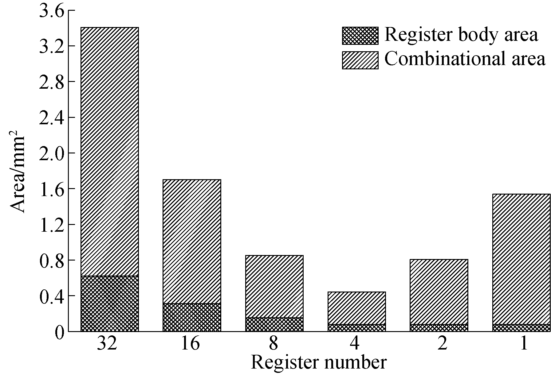
Fig.2 The relationship of the number of register files and area trend
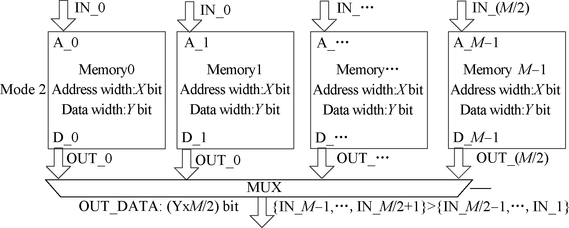
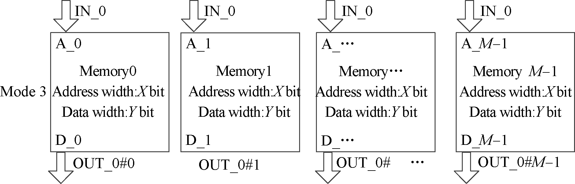
Meanwhile, the register file designed in this paper supports run-time reconfiguration to meet the demands of various access types. By changing the configuration, three operation modes can be easily realized as shown in Fig.3.
Mode1 The input width isXwhile the output width isY. This mode can fulfill the scenario when the input and output width of the register are less thanXandY, respectively.
Mode2 The input width is (X+log2(ceil(M/2))) while the output width is (X+log2(ceil(M/2))). This mode specifically targets the scenario that the register capacity is not large enough.
Mode3 The input width isXwhile the output width isYM. The register is regarded as anX-entryYM-bit memory.
According to different computing scenarios of GRF and LRF, different architectures of the register file are proposed in this paper.

(a)
(b)
(c)
Fig.3 Data input and output schematic.(a) Mode 1; (b) Mode 2; (c) Mode 3
2.2 Design of local register file
LRF is used to realize the S-box in the block cipher, of which the capacity and parallel access ports should meet the demands of each block cipher. In this paper, each group of LRF contains four 32-port 8-entry 8-bit registers. As shown in Fig.4, 2 bits are used to configure the LRF among different modes.
The details of the input and output controller of LRF are shown in Fig.5 and Fig.6. The four input data IN-A, IN-B, IN-C and IN-D are assembled as one 32-bit data in Mode 1, while in Mode 2 and Mode 3 only IN-A is expanded to a 32-bit data.
The output controller combines the output data D0, D1, D2 and D3 of the register body into a 32-bit data in Modes 1 and 3. While in Mode 2, they are combined into two 16-bit data.
2.3 Design of global register file
The greater the capacity of GRF, the higher the performance of the cryptographic processor will be. However, the area cost increases rapidly while the capacity of GRF grows slower relatively. Therefore, performance benefits from GRF and the area overhead caused by it should be considered comprehensively.
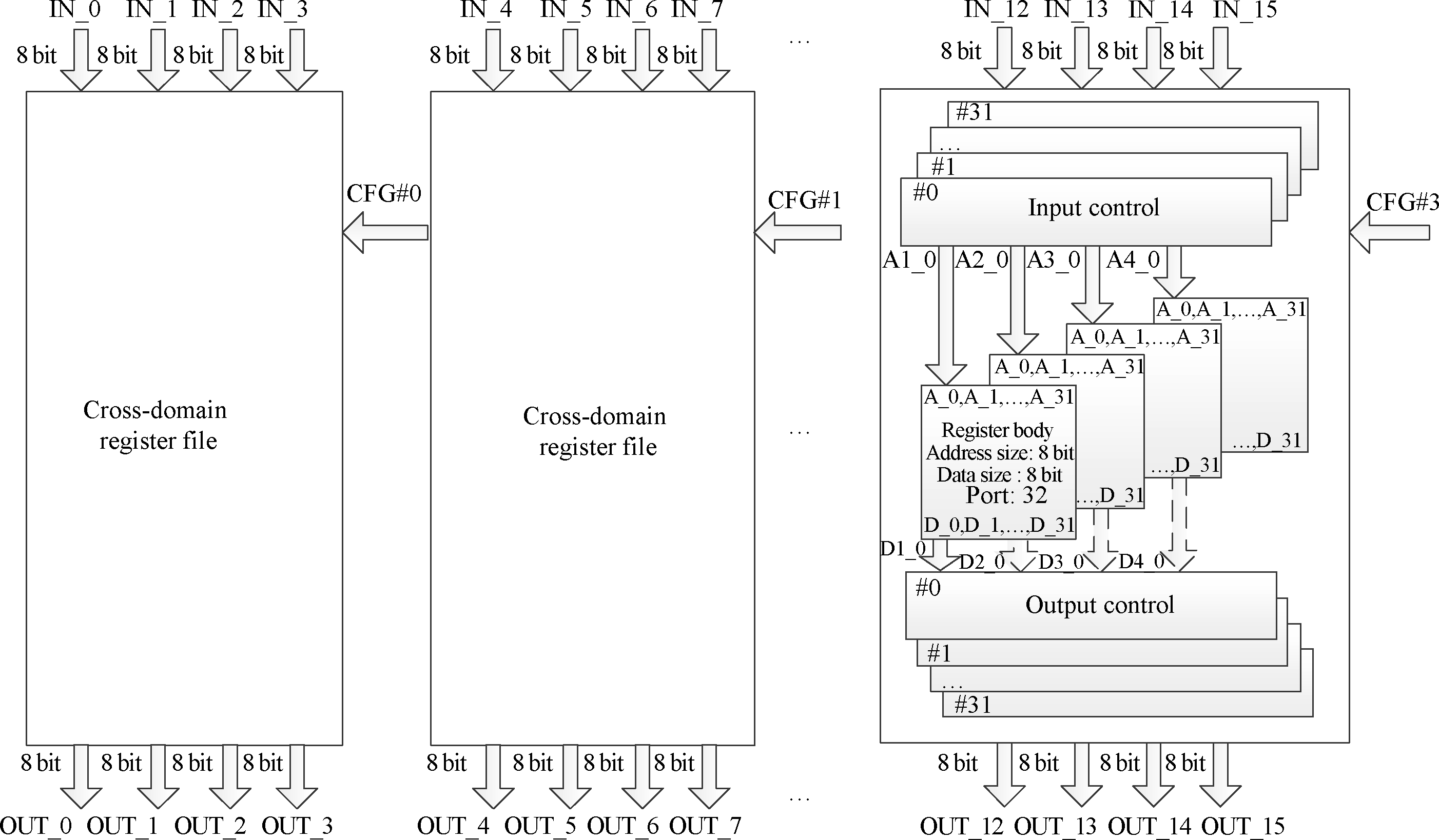
Fig.4 Schematic diagram of local register file
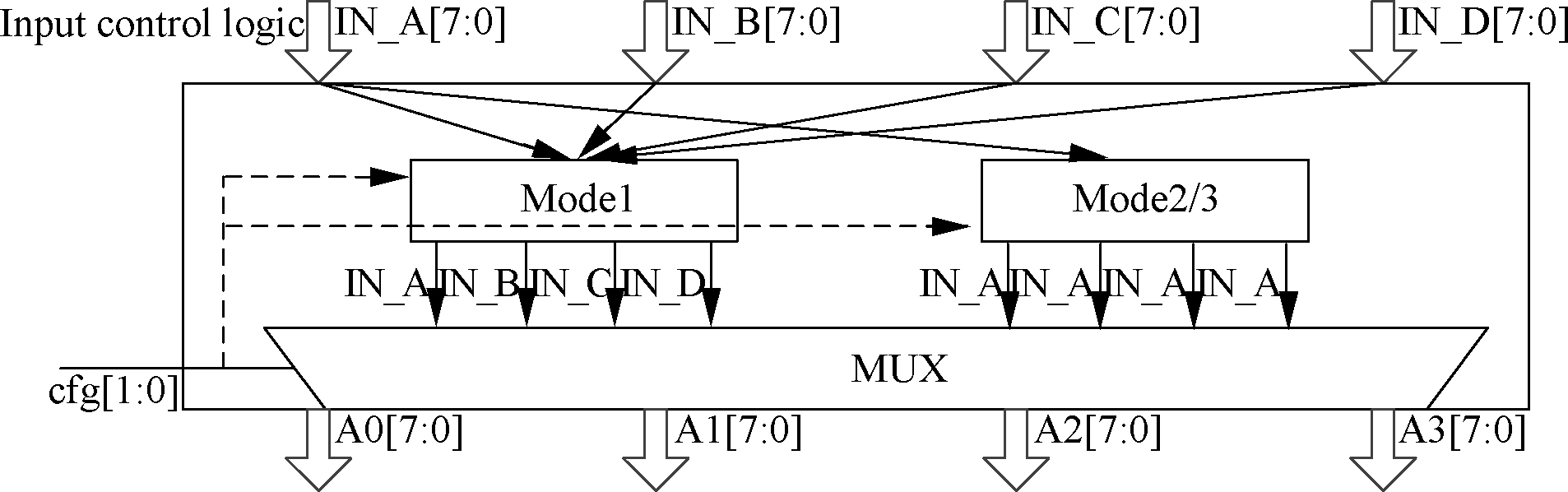
Fig.5 Schematic diagram of input control logic
As is depicted in Fig.7, The GRF proposed in this paper contains a 20-read-port, 2-write-port register file. Each register file is formed by a 20-port 7-entry 32-bit memory and 20 input/output controllers. The even lines ofthe processor are connected to the 20 ports, while line 19 and 39 are connected to the two write ports. The input and output controllers in GRF only need to support Mode 1.
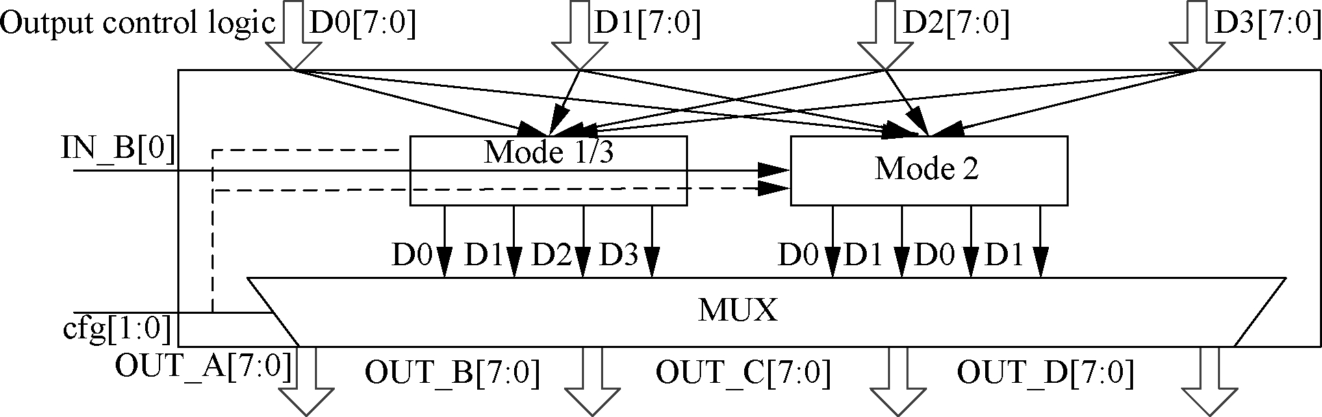
Fig.6 Schematic diagram of output control logic
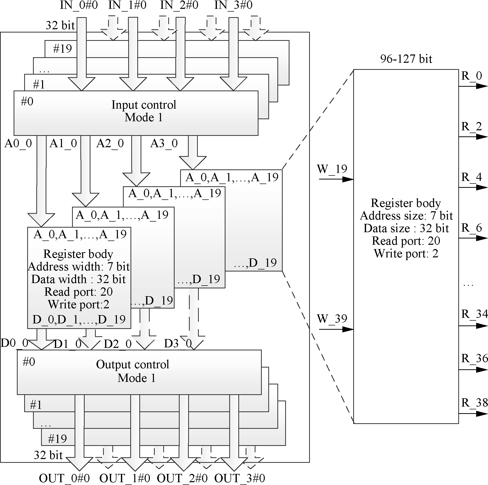
Fig.7 Schematic diagram of global register file
In order to efficiently carry out experiment analysis for the optimized results of the distributed cross-domain register file architecture, this paper adopts the same architecture framework of the Cryptoraptor cryptographic processor including the reconfigurable array size, reconfigurable cell unit and the sub-operation behavior of the block cipher. The proposed global register files and local register files are taken to replace the same modules in the Cryptoraptor. Both kinds of global register files and local register files are implemented under the TSMC 40 nm CMOS processing and the area information is obtained by the synthesis tools of the design compiler.
3.1 Comparative analysis of area overhead
The GRF of the proposed design uses four register bodies of 128 entries and 32-bit data width. Each register body is designed with 20 ports. For comparison, the Cryptoraptor adopts a register body of 256 entries and 32-bit data width.
In terms of LRF, our design adopts 32 register bodies of 256 entries with 8-bit data width, and each register body needs to provide 32 ports to meet the parallel access requirement. For comparison, the Cryptoraptor adopted three signal port register bodies of 256 entries and 32-bit data width and a signal port register bodies of 1 024 entries with 32-bit data width.
From the area comparison results of register files shown in Tab.1, the capacity of the proposed global register files is doubled, but the area overhead decreases by 42.63%. This is due to the proposed register file architecture design method which reduced the combination decoder logic area overhead.
For the local register files, the proposed design capacity reduced down to 97.14% and the area overhead decreased by 40.15%. This is because under the same demand of the block cipher algorithm set, the proposed design meets the concurrent access requirements by increasing the port number but not the register capacitance. It should be further noted that the Cryptoraptor adopted the CASTI model to estimate the TLU area of 0.88 mm2for the lack of the register compiler. In our experiments, we adopted the register compiler of 40 nm low power design and development tools of artisan by ARM to generate high-density signal port register files. By this method, the local register files area of the Cryptoraptor is 2.54 mm2.
Tab.1 Area comparison of different register file architectures
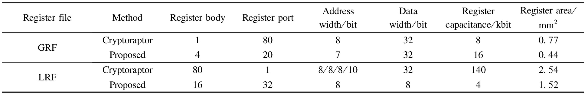
RegisterfileMethodRegisterbodyRegisterportAddresswidth/bitDatawidth/bitRegistercapacitance/kbitRegisterarea/mm2GRFCryptoraptor1808328077Proposed42073216044LRFCryptoraptor8018/8/8/1032140254Proposed1632884152
3.2 Comparative analysis of unit area performance
The implementation of the block cipher algorithm on the coarse-grained reconfigurable process is the process of the cryptographic algorithm round function mapped on reconfigurable array, which can efficiently improve the execution parallelism and reduce run time by the software pipeline computation method. The key index of performance can be evaluated by block per cycle(block/cycle) and block per cycle per area((block·cycle-1)/area).
The block per cycle characterizes the performance of parallel computing, which is determined by the number of blocks and the execution cycles. The block per cycle per area is an indicator to characterize computing performance per unit area, which is determined by the block per cycle and the area. Block is the total number of plaintext data. Cycle is the number of execution cycles. Since the number of blocks is determined, the key issues of optimizing block per cycle and block per cycle per area are to reduce the cycle and area.
Tab.2 shows the comparison of the algorithm performance and contrasts of area efficiency between different register file architectures. Since more storage space of the global register file reduces computing pause, the proposed cross-domain distributed register file architecture design method can achieve an average performance of 0.60 block/cycle. Compared with the average performance of 0.49 block/cycle by the Cryptoraptor, the proposed design method increases the performance by 17.79%. Thanks to the gains in area, the proposed cross-domain distributed register file architecture design method can achieve efficiency of performance per unit area 0.31(block·cycle-1)/area. Compared to 0.15 (block·cycle-1)/area of the Cryptoraptor, the proposed design method obtains an average profit of 117% improvement. Wherein, the performance of the AES algorithm does not change. So, the area efficiency increasing 68.72% benefits from the area reduction. The KASUMI algorithm simultaneously benefits from the performance increasing and the area reduction, which achieves the largest area efficiency of 237.43%.
Tab.2 Performance and area comparison of different register file programs
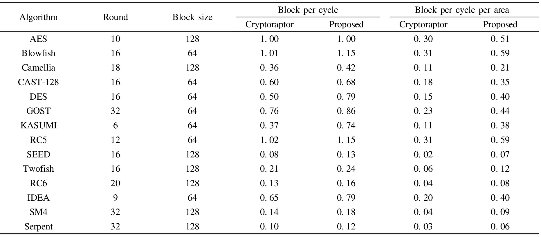
AlgorithmRoundBlocksizeBlockpercycleBlockpercycleperareaCryptoraptorProposedCryptoraptorProposedAES10128100100030051Blowfish1664101115031059Camellia18128036042011021CAST⁃1281664060068018035DES1664050079015040GOST3264076086023044KASUMI664037074011038RC51264102115031059SEED16128008013002007Twofish16128021024006012RC620128013016004008IDEA964065079020040SM432128014018004009Serpent32128010012003006
This paper presents a novel distributed cross-domain register file architecture. With the proposed design, the reconfigurable cryptographic processor global registers and local registers meet the design requirements under the restraint constraints of different sets of algorithms and reconfigurable frameworks. By implementation and comparative analysis, the proposed architecture achieves double the capacity of global register files, meanwhile effectively reducing the area overhead down to 42.63%. Under the same condition of the block cipher algorithm set, the area of local registers files is decreased by up to 40.15%. The performance of the targeted block cipher algorithm set increased at an average rate of 17.79%. Meanwhile, the area efficiency achieved 117% improvement with the limited capacity of the reconfigurable array.
[1]Liu B, Baas B M. Parallel AES encryption engines for many-core processor arrays[J].IEEETransactionsonComputers, 2013,62(3):536-547. DOI:10.1109/tc.2011.251.
[2]Yan M, Yang Z Y, Liu L, et al. ProDFA: Accelerating domain applications with a coarse-grained runtime reconfigurable architecture[C]//IEEE18thInternationalConferenceonParallelandDistributedSystems(ICPADS). Singapore, 2012:834-839. DOI: 10.1109/ICPADS.2012.136.
[3]Li H, Ding J, Pan Y. Cell array reconfigurable architecture for high-efficiency AES system[J].MicroelectronicsReliability, 2012,52(11): 2829-2836. DOI:10.1016/j.microrel.2012.04.020.
[4]Wang M Y, Su C P, Horng C L, et al. Single- and multi-core configurable AES architectures for flexible security[J].IEEETransactionsonVeryLargeScaleIntegrationSystems, 2010,18(4): 541-552. DOI:10.1109/tvlsi.2009.2013231.
[5]Bertoni G M, Breveglieri L, Roberto F, et al. Speeding up AES by extending a 32 bit processor instruction set[C]//InternationalConferenceonApplication-SpecificSystems,ArchitecturesandProcessors. Steamboat Springs, CO, USA, 2006:275-282. DOI: 10.1109/ASAP.2006.62.
[6]Mathew S K, Sheikh F, Kounavis M, et al. 53 Gbps native GF(24)2 composite-field AES-encrypt/decrypt accelerator for content-protection in 45 nm high-performance microprocessors[J].IEEEJournalofSolid-StateCircuits, 2011,46(4):767-776. DOI:10.1109/jssc.2011.2108131.
[7]Dai Z, Li W, Meng T, et al. The research and design of parallel instruction targeted at substitution box[C]//IEEE8thInternationalConferenceonASIC. Changsha, China, 2009: 155-158. DOI: 10.1109/ASICON.2009.5351585.
[8]Sayilar G, Chiou D. Cryptoraptor: High throughput reconfigurable cryptographic processor[C]//Proceedingsofthe2014IEEE/ACMInternationalConferenceonComputer-AidedDesign. San Jose, CA, USA, 2014: 154-161.
[9]Shan W W, Zhang X, Fu X Y, et al. VLSI design of a reconfigurable s-box based on memory sharing method[J].IEICEElectronExpress, 2014,11(1): 20130872. DOI:10.1587/elex.10.20130872.
[10]Singh H, Lee M H, Lu G M, et al. MorphoSys: An integrated reconfigurable system for data-parallel and computation-intensive applications[J].IEEETransactionsonComputers, 2000,49(5): 465-481. DOI:10.1109/12.859540.
References
摘要:由于寄存器文件严重影响可重构密码处理器的性能和面积,为了实现高性能和低面积消耗的密码处理器,提出了一种高效的分布式跨域寄存器结构.通过分析不同分组密码的算法特点,设计了统一的多端口访问结构——分布式跨域寄存器文件.针对全局寄存器文件和局部寄存器文件不同的算法需求,在TSMC 40 nm CMOS工艺下,采用不同设计参数分别完成电路实现并与类似结构做比较.实验结果显示,所提出的分布式跨域寄存器结构能够有效地提升单位面积的性能,其中单位时间分组密码性能提升了17.79%,单位面积时间分组密码性能提升了117%.
关键词:可重构处理器;分组密码;并行实现;寄存器文件
中图分类号:TP302
![]()
JournalofSoutheastUniversity(EnglishEdition) Vol.33,No.3,pp.266⁃272Sept.2017 ISSN1003—7985
DOI:10.3969/j.issn.1003-7985.2017.03.002
Foundationitem:The National Natural Science Foundation of China (No.61176024).
Citation:Zhang Baoning, Ge Wei, Wang Zhen.A distributed cross-domain register file for reconfigurable cryptographic processor[J].Journal of Southeast University (English Edition),2017,33(3):260-265.
DOI:10.3969/j.issn.1003-7985.2017.03.002.