With the exponential growth in high speed transmission, electrical interconnection has encountered a bottleneck for the skin effect, dielectric loss, and channel cross-talk noises[1].As an alternative method to replace electrical interconnection, optical interconnection has attracted more and more attention.Optoelectronic integrated circuit receivers fabricated by standard CMOS technology have become such a huge trend in optical interconnects for their high cost-efficiency[2-3].
For an optical receiver, the photodetector converts the optical signal into a current signal, and then the current signal is amplified and transformed into a voltage signal by a trans-impedance amplifier (TIA).To achieve a photodetector with high responsivity, the area of the photodetector should be as large as possible, but that will make its parasitic capacitance large.However, large parasitic capacitance will have an impact on the bandwidth of the entire receiver.
Various techniques have been proposed to relax this bandwidth limitation.For example, inductive-peaking TIAs[4-5] and regulated-cascode (RGC)TIAs and their modifications[6-9] are widely used to enhance receiver bandwidths.RGC TIAs can effectively boost the bandwidth, but the intrinsic characteristics limit the performance.The inductive-peaking technology is another way to improve the bandwidth at the expense of voltage headroom and area consumption.Therefore, the challenge in designing TIAs is making a trade-off among bandwidth, area and power consumption.
In our OEIC system, a deep-N-well-strip-spatially-modulated photodetector (DNW-strip-SMPD)operating in an avalanche mode has been designed and tested.The parasitic capacitance is around 830 fF, and the responsivity is 1.4 A/W.Therefore, in this paper, a compact, low power and wide bandwidth TIA is proposed for the OEIC system.
1 Circuit Design and Analysis
1.1 Design of DNFFCG TIA
Fig.1 shows the schematic of the DNFFCG TIA with a differential structure.The parasitic capacitance of the input node is a very large value compared with other nodes of the TIA circuit.Owing to these input parasitic capacitance components, the only way to improve the 3-dB bandwidth is to decrease the input resistance.
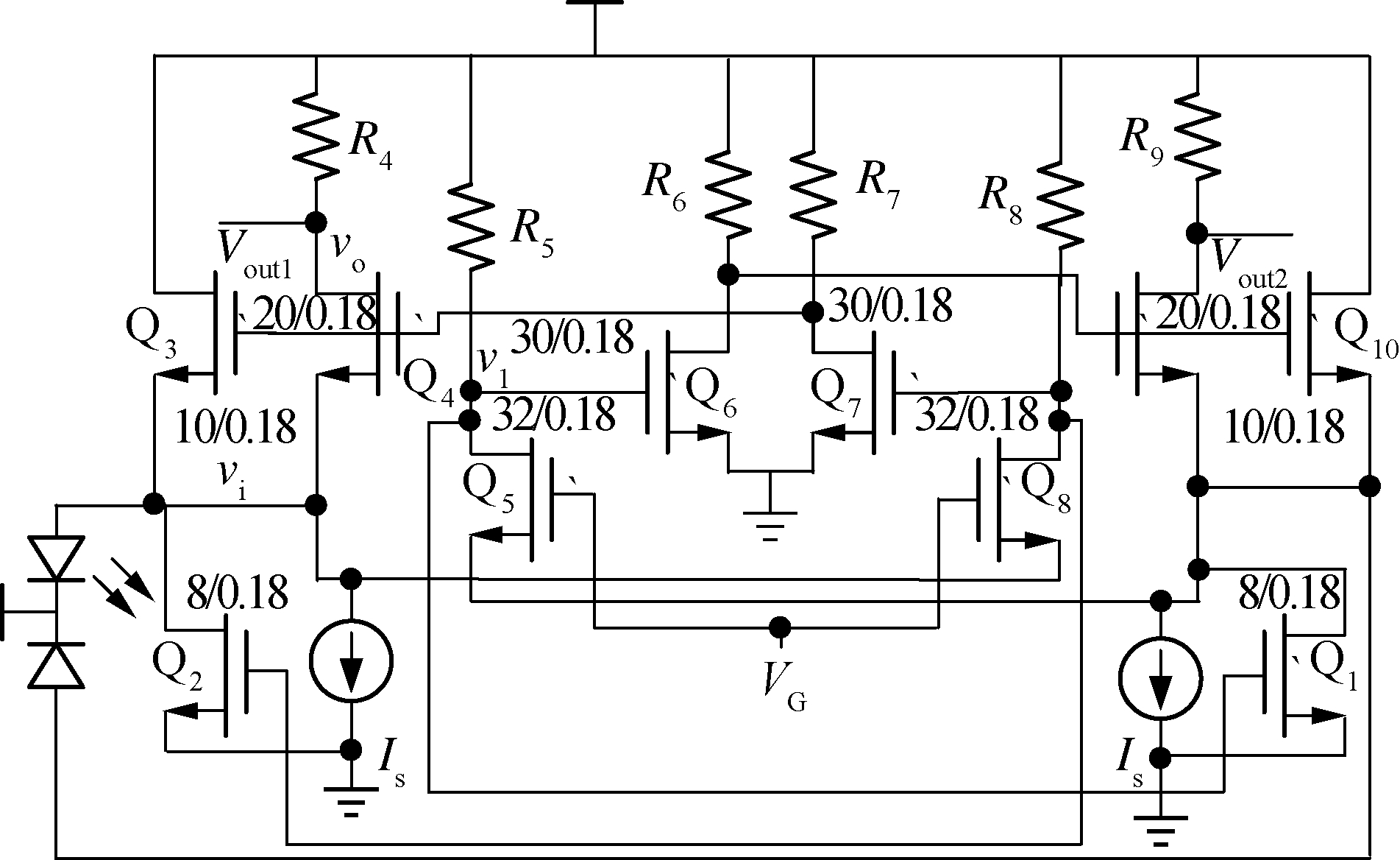
Fig.1 The schematic diagram of DNFFCG differential TIA
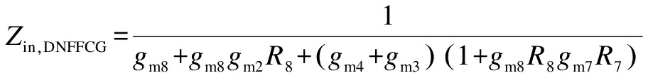
For the TIAs with common-gate topology, by increasing gm, the input resistance can be reduced, but this will consume large amounts of power.Gain-boost technology is proposed with a large feedback gain to obtain enough equivalent gm in the case of small gm4/gm9.In this design, a local feedback stage is employed, consisting of Q8/Q5, R8/R5, Q7/Q6 and R7/R6.Besides, to further reduce the input resistance, two negative feedback loops are also designed.The first negative feedback loop is composed of Q3/Q10, Q8/Q5, R8/R5, Q7/Q6 and R7/R6.The other negative feedback loop comprises Q2/Q1, Q8/Q5 and R8/R5.The input resistance of the DNFFCG differential TIA can be expressed as
(1)
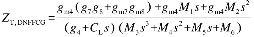
It can be seen from Eq.(1)that the resistance can be reduced by increasing gm2, gm3 or the local feedback gain.Fig.2 shows the equivalent small-signal model of the DNFFCG TIA circuit to analyze poles and zeros.According to the Miller Theorem, Cgs3 and Cgs4 have been de-coupled between node 1 and 2.By solving the small-signal model equations, the approximate transfer function of DNFFCG TIA can be derived:
(2)
where
M1=g8(Cgs4+Cgs3)+g7(Cgs7+Cgs2)
M2=(Cgs4+Cgs3)(Cgs7+Cgs2)
M3=(Cgs4+Cgs3)(Cgs7+Cgs2)(Cgs8+Cin+k(Cgs4+Cgs3))
M4=[(Cgs4+Cgs3)(Cgs7+Cgs2)(gm4+gm8+gm3)+
(Cgs8+Cin+k(Cgs4+Cgs3))][g8(Cgs4+Cgs3)+
g7(Cgs7+Cgs2)]
M5=(gm4+gm8+gm3)[g8(Cgs4+Cgs3)+g7(Cgs7+Cgs2)]+
g7g8(Cgs8+Cin+k(Cgs4+Cgs3))+gm2gm8(Cgs4+Cgs3)
M6=(gm4+gm8+gm3)g7g8+(gm3+gm4)gm7gm8+g7gm2gm8
Where, g7, g8, and g4 are the conductance of R7, R8, and R4, respectively; CL is the equivalent loading capacitance at the output node coming from the secondary circuit; k is the equivalent miller factor of Cgs3 and Cgs4.In order to facilitate the analysis, the equation needs to be simplified as
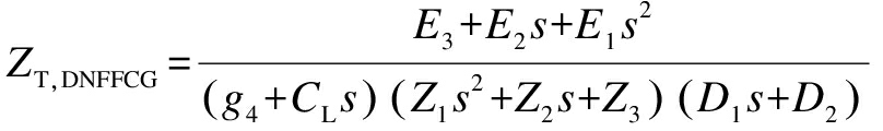
(3)
where
E1=gm4(Cgs4+Cgs3)(Cgs7+Cgs2)
E2=gm4[g8(Cgs4+Cgs3)+g7(Cgs7+Cgs2)]
E3=gm4(g7g8+gm7gm8)
D1=Cgs8+Cin+k(Cgs4+Cgs3)=Cin,tot

Z1=(Cgs4+Cgs3)(Cgs7+Cgs2)
Z2≈{(gm4+gm8+gm3)[g8(Cgs4+Cgs3)+g7(Cgs7+Cgs2)]+
gm2g8(Cgs4+Cgs3)}Zin
Z3=g7g8
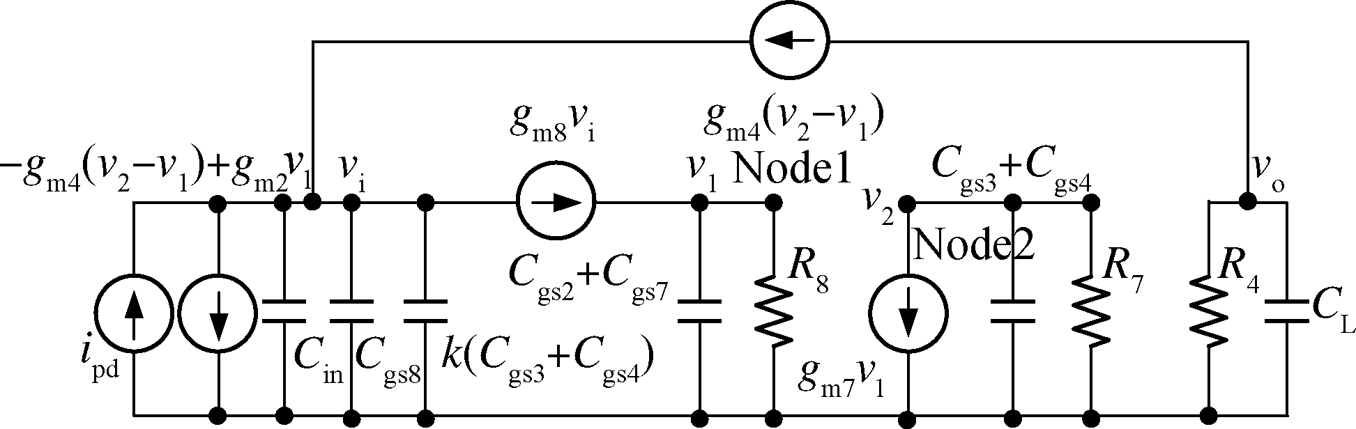
Fig.2 Equivalent small-signal model for DNFFCG TIA circuit
For a typical complex-pole system ![]() the frequency response of the complex poles can be characterized by the damping coefficient
the frequency response of the complex poles can be characterized by the damping coefficient ![]() When ξpoles >1, the circuit response speed will slow down with the increase of ξpoles, which will cause the eye diagram to not open.The maximal flat response will be obtained for ξpoles=0.707, while there is no bandwidth expansion effect.When 0 <ξpoles<0.707, the amplitude response will have a peak, which will extend the bandwidth to some extent.The bandwidth expansion rate can be improved with the decrease of ξpoles.However, ξpoles cannot be too small, otherwise it will cause excessive gain overshoot, longer settling time and smaller phase linear range.In this design, there is a trade-off among the bandwidth extension, the gain overshoot, and settling time, and finally ξpoles is chosen to be 0.3.In addition, two complex zeros in the denominator should be designed carefully.The complex zeros are arranged near the dominant pole, which can also play the role of expanding the bandwidth.The frequency responses of the complex zeros are opposite to the complex poles.To balance these two contrary effects,
When ξpoles >1, the circuit response speed will slow down with the increase of ξpoles, which will cause the eye diagram to not open.The maximal flat response will be obtained for ξpoles=0.707, while there is no bandwidth expansion effect.When 0 <ξpoles<0.707, the amplitude response will have a peak, which will extend the bandwidth to some extent.The bandwidth expansion rate can be improved with the decrease of ξpoles.However, ξpoles cannot be too small, otherwise it will cause excessive gain overshoot, longer settling time and smaller phase linear range.In this design, there is a trade-off among the bandwidth extension, the gain overshoot, and settling time, and finally ξpoles is chosen to be 0.3.In addition, two complex zeros in the denominator should be designed carefully.The complex zeros are arranged near the dominant pole, which can also play the role of expanding the bandwidth.The frequency responses of the complex zeros are opposite to the complex poles.To balance these two contrary effects, ![]() is chosen to be 0.35.
is chosen to be 0.35.
Fig.3 shows the pre-simulation AC curves of the DNFFCG differential TIA with the different input parasitic capacitance.The 3-dB bandwidths of 730, 830 and 930 fF are 9.9, 9.5 and 8.9 GHz, respectively.
1.2 Noise analysis
For the entire optical receiver, the noise of the frontend TIA is usually the dominant contributor to the input referred noise.The total equivalent input noise current spectral density of the TIA is derived by analyzing the equivalent input noise contributed by each noise sources.
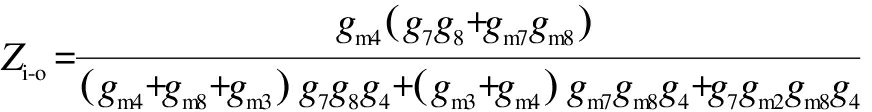
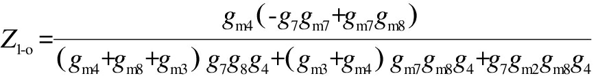
First, the low frequency trans-impedance gain from each node to the output needs to be derived:
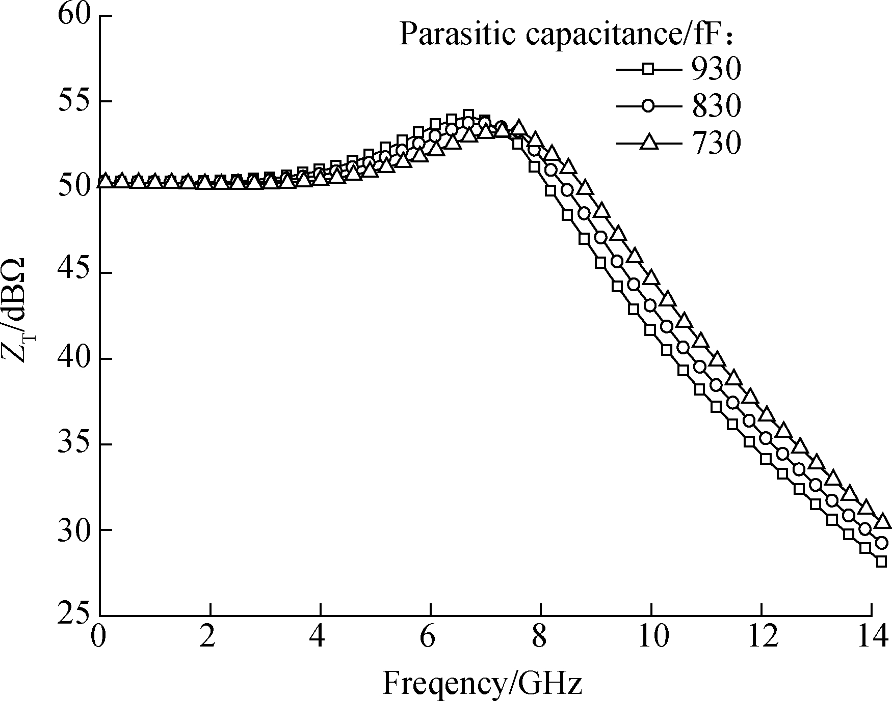
Fig.3 The pre-simulation AC curves of the DNFFCG TIA
(4)
(5)
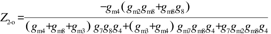
(6)
Zo-o=g4
(7)
The overall input noise current spectral density can be evaluated as
(8)
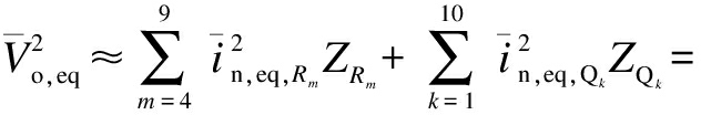
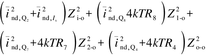
where in,eq,Qk is the drain noise current of transistor Qk; in,eq,Rm is the thermal noise current of resistor Rm; and ZRm and ZQk are the trans-impedance gain between corresponding nodes and output.The total average equivalent input noise current can be expressed as
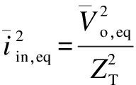
(9)
As the values of R4, R7 and R8 are relatively high, the thermal noise from these resistances cannot be the major contributors.Theoretically speaking, Q8/Q5 contributes most to the total noise-current spectral density.Therefore, the W/L of Q8/Q5 needs to be optimized.Fig.4 shows the pre-simulation results of the average equivalent input noise current densities at different W/L of Q8/Q5.The average equivalent input noise current densities will decrease by increasing the W/L of Q8/Q5.However, the Cgs of Q8/Q5 will be large, and it will have an impact on the bandwidth.Finally, the W of Q8/Q5 is chosen to be 32 μm.Besides, Q3/Q10 and Q2/Q1 are introduced to further reduce the input resistance, but it will increase the noise and decrease sensitivity.The average equivalent input noise current densities are increased by 6 pA/Hz1/2 by simulation.The sensitivity S can be calculated by[10]
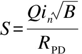
(10)
where Q is the theoretical factor; B is the bandwidth of the TIA; and RPD is the responsivity of the photodetector.As the responsivity of the DNW-strip-SMPD is larger than most of the photodetectors fabricated by CMOS technology, it can reduce the influence of the noise current densities on sensitivity.Also, it is more important to achieve a large bandwidth in the case of the large parasitic capacitance of the photodetector, so appropriate sacrifice of noise current densities is acceptable.For BER=10-12, Q=7 and the theoretical calculation of sensitivity is approximately -33 dBm.
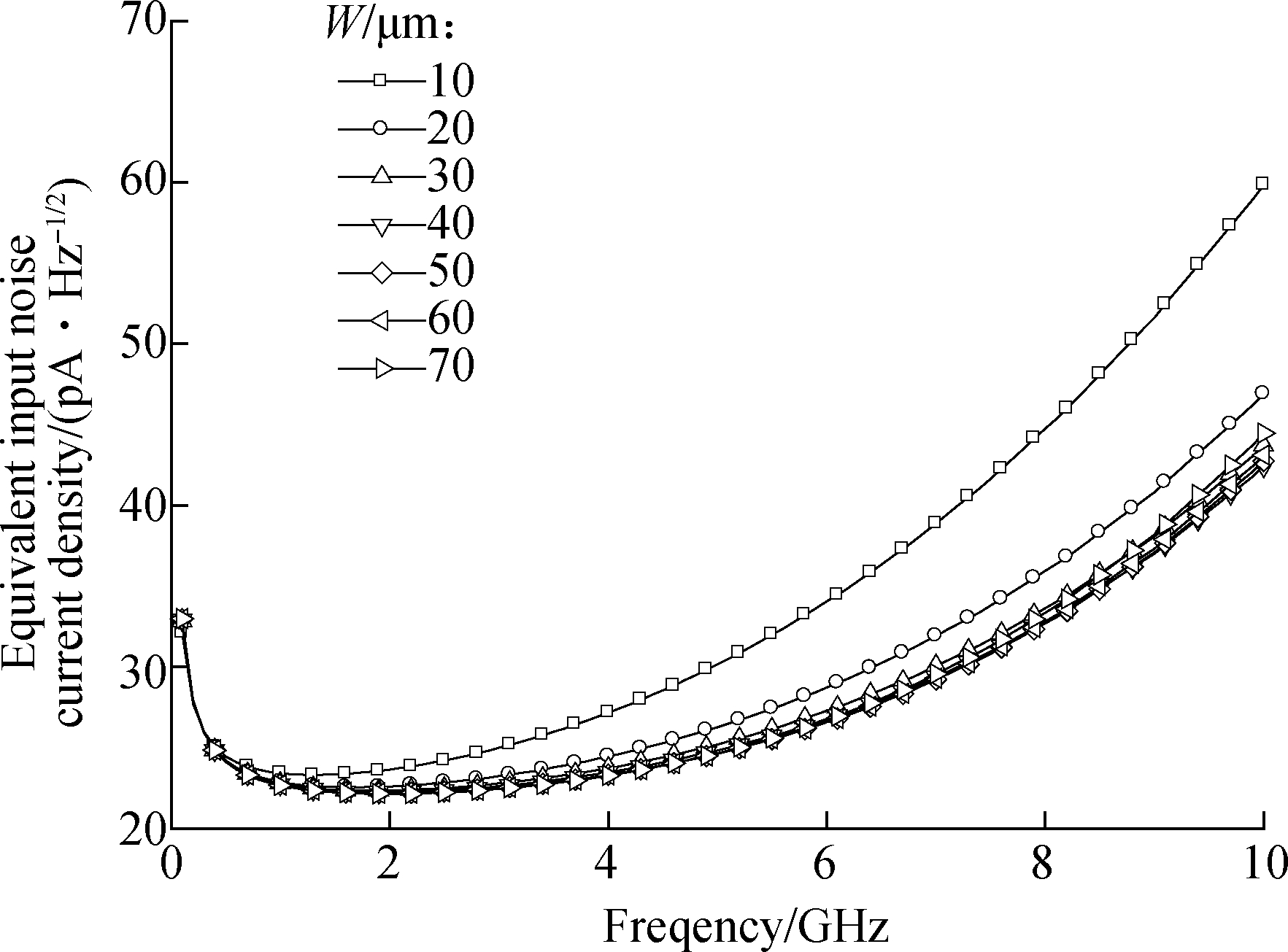
Fig.4 The pre-simulation results of the average equivalent input noise current densities at different W of Q8/Q5
2 Implementation and Measurement Result
The chip micrograph of the proposed circuit and the diagram of the measurement setup are shown in Fig.5 and Fig.6, respectively.The chip area is 0.45×0.49 mm2 including all pads, while the core area is 0.06×0.06 mm2.At the bias condition of unified 1.8-V VDD, 1.1-V VG, the proposed circuit consumed 24.2 mW power including 2-stage differential buffers, while DNFFCG stages consumed 14.6 mW.
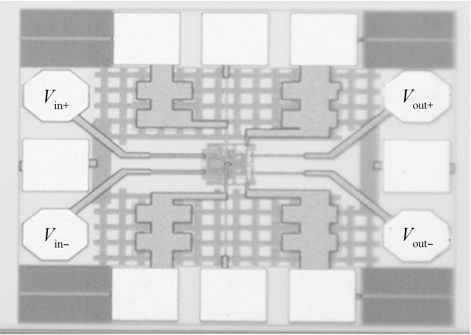
Fig.5 The chip micrograph of the proposed circuit

Fig.6 Measurement setup
The test 3-dB bandwidth and gain are shown in Fig.7, as well as the simulated 3-dB bandwidth and gain.The test 3-dB bandwidth of the proposed DNFFCG TIA is 9 GHz and the test transimpedance gain is 49.2 dBΩ.Fig.8 shows the simulated and measured average equivalent input noise current densities.The measured average equivalent input noise current density is 28.1 pA/Hz1/2.As the test environment will affect the test result, the results of the measured average equivalent input noise current densities are larger than the simulation results.Besides, the measured minimum input peak-to-peak voltage is 5 mV.
Fig.7 The post simulated and measured frequency responses of the proposed TIA
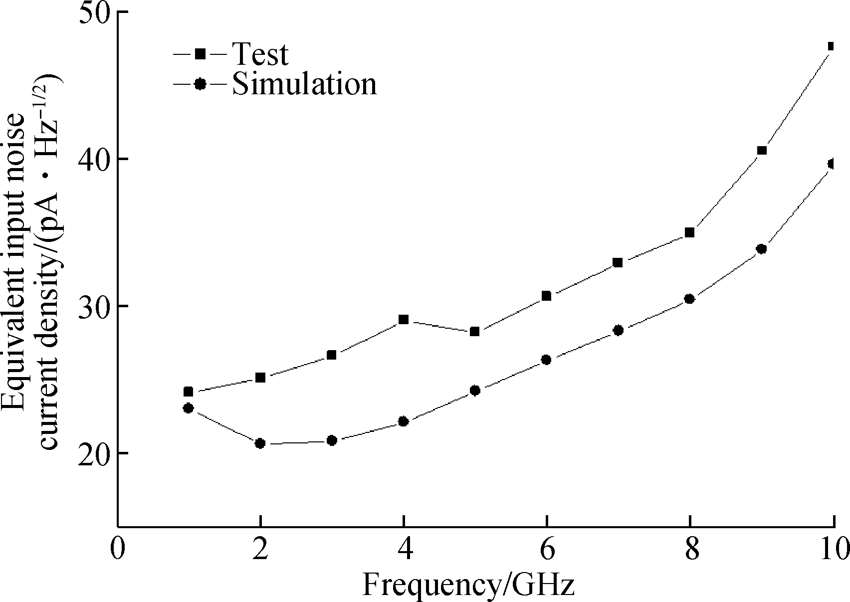
Fig.8 The post simulated and measured average equivalent input noise current densities
The figure of merit (FoM)is defined as
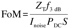
(11)
where ZT is the transimpedance gain; f3 dB is the 3 dB bandwidth; Inoise is the average equivalent input noise current density; PDC is the power consumption; S is the core area of the chip.FoM of the DNFFCG differential TIA is calculated to be 299.8.The proposed work shows superiority in terms of FoM.In addition, the output eye diagrams measured are shown in Fig.9 with a 223-1 pseudorandom bit sequence input data at frequencies of 10 and 12 Gbit/s (Vin-pp=20 mV).
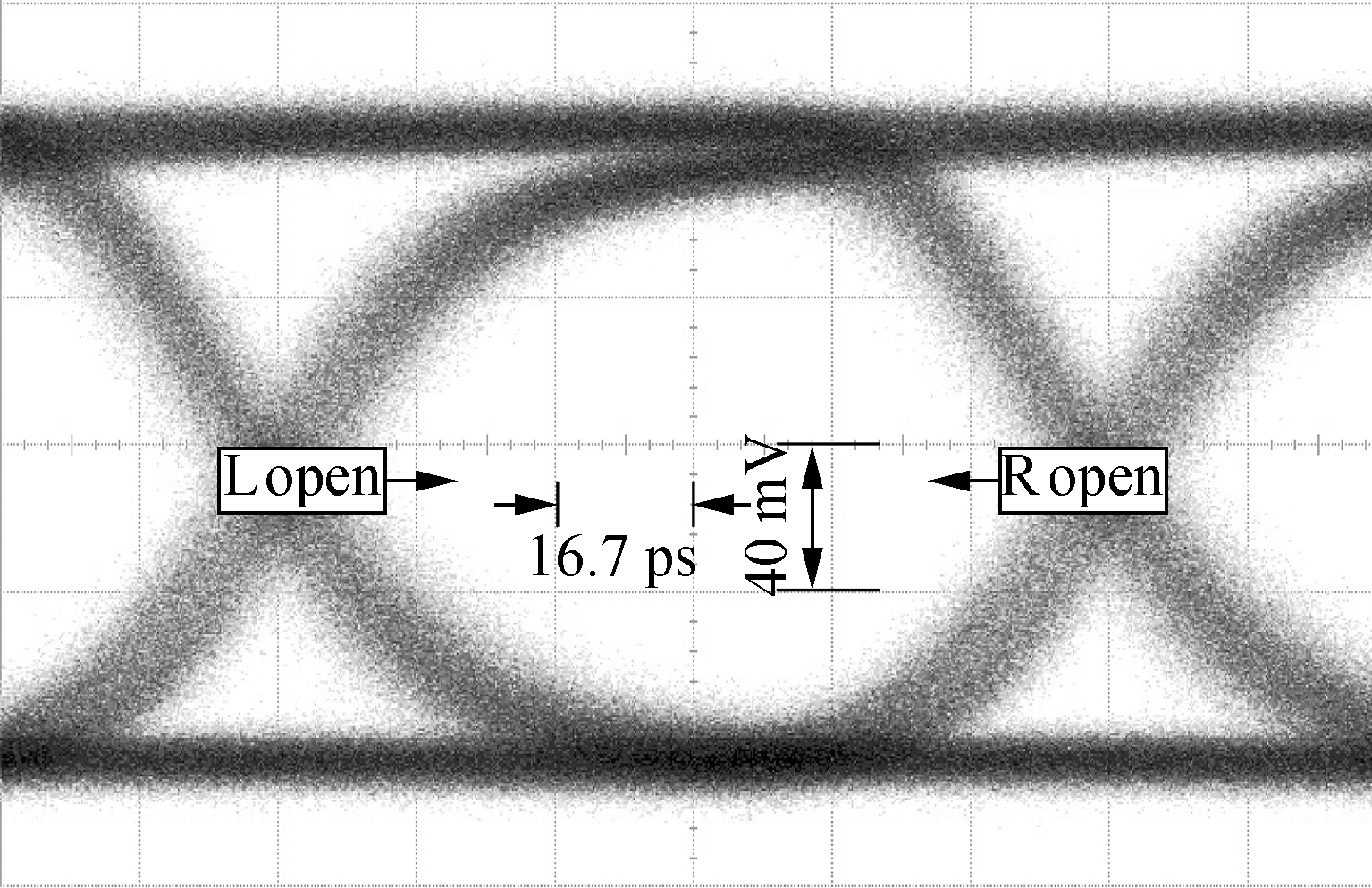
(a)

(b)
Fig.9 Output eye-diagram of the proposed preamplifier with 231-1 PRBS NRZ input data.(a)10 Gbit/s;(b)12 Gbit/s
Tab.1 shows a summary of the implemented CMOS UWB TIA, and recently reported state-of-the-art CMOS UWB TIAs.As can be seen, compared with other works, it exhibits the highest FOM.Moreover, if the difference of manufacturing costs between these processes is taken into account, the performance-to-cost ratio of this work is in the first class.
3 Conclusion
A DNFFCG differential TIA fabricated in a 0.18 m CMOS process is proposed for the VSR OEIC system in this paper.Moreover, the transmission rate of 12 Gbit/s can be achieved with a very small chip area and low consumption power.Measured results demonstrate that the TIA has a transimpedance gain of 49.2 dBΩ with a 3 dB bandwidth of 9 GHz.The measured average equivalent input noise current density is 28.1 pA/Hz1/2.The DNFFCG differential TIA can be applied to low cost, low power and high speed optical communication systems.
Tab.1 Performance comparison of CMOS UWB TIA
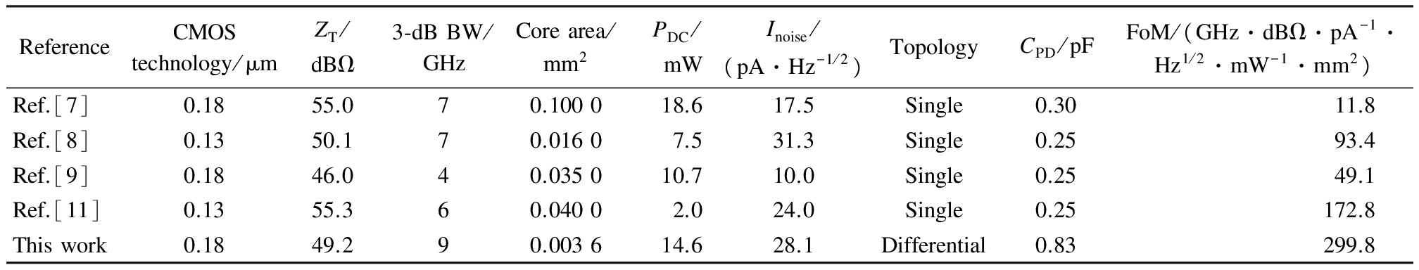
ReferenceCMOStechnology/μmZT/dBΩ3⁃dBBW/GHzCorearea/mm2PDC/mWInoise/(pA·Hz-1/2)TopologyCPD/pFFoM/(GHz·dBΩ·pA-1·Hz1/2·mW-1·mm2)Ref.[7]0.1855.070.100018.617.5Single0.3011.8Ref.[8]0.1350.170.01607.531.3Single0.2593.4Ref.[9]0.1846.040.035010.710.0Single0.2549.1Ref.[11]0.1355.360.04002.024.0Single0.25172.8Thiswork0.1849.290.003614.628.1Differential0.83299.8
References
[1]Miller D.Device requirements for optical interconnects to silicon chips[J].Proceedings of the IEEE, 2009, 97(7): 1166-1185.DOI:10.1109/jproc.2009.2014298.
[2]Huang S H, Chen W Z, Chang Y W, et al.A 10-Gb/s OEIC with meshed spatially-modulated photo detector in 0.18-μm CMOS technology [J].IEEE Journal of Solid-State Circuits, 2011, 46(5):1158-1169.DOI: 10.1109/JSSC.2011.2116430.
[3]Pan Q, Hou Z X, Li Y, et al.A 0.5-V P-well/Deep N-well photodetector in 65-nm CMOS for monolithic 850-nm optical receivers [J].IEEE Photonics Technology Letters, 2014, 26(12):1184-1187.
[4]Wu C H, Lee C H, Chen W S, et al.CMOS wideband amplifiers using multiple inductive-series peaking technique[J].IEEE Journal of Solid-State Circuits, 2005, 40(2):548-552.
[5]Analui B, Hajimiri A.Bandwidth enhancement for transimpedance amplifiers[J].IEEE Journal of Solid-State Circuits, 2004, 39(8): 1263-1270.DOI:10.1109/jssc.2004.831783.
[6]Lu Z, Yeo K S, Lim W M, et al.Design of a CMOS broadband transimpedance amplifier with active feedback[J].IEEE Transactions on Very Large Scale Integration (VLSI)Systems, 2010, 18(3): 461-472.DOI:10.1109/tvlsi.2008.2012262.
[7] Ahmadi P, Haslett, J W, Belostotski L, et al.10-Gb/s 0.13-CMOS inductorless modified-RGC transimpedance amplifier [J].IEEE Transactions on Circuits and Systems-Ⅰ-Regular Papers,2015, 62(8):1971-1980.
[8]Chen D, Yeo K S, Shi X, et al.Cross-coupled current conveyor based CMOS transimpedance amplifier for broadband data transmission[J].IEEE Transactions on Very Large Scale Integration (VLSI)Systems, 2013, 21(8):1516-1525.DOI:10.1109/tvlsi.2012.2211086.
[9]Momeni O, Hashemi H, Afshari E.A 10-Gb/s inductorless transimpedance amplifier[J].IEEE Transactions on Circuits and Systems Ⅱ: Express Briefs, 2010, 57(12): 926-930.DOI:10.1109/tcsii.2010.2087971.
[10] Gu G W, Zhu E, Lin Y.Design of 10 Gbit/s burst-mode transimpedance preamplifier for PON system [J].Journal of Southeast University (English Edition), 2012, 28(4):398-403.
[11]Taghavi M H, Belostotski L, Haslett J W.A CMOS low-power cross-coupled immittance-converter transimpedance amplifier[J].IEEE Microwave and Wireless Components Letters, 2015, 25(6): 403-405.DOI:10.1109/lmwc.2015.2421253.