The advent of the three-dimensional integrated circuit (3D IC) technology has opened up the potential of highly improved circuit designs. Through-silicon vias (TSVs) enable the vertical integration of separate dies to form a single 3D chip. The TSV-based 3D stacking technology promises better performance, including a smaller footprint, higher bandwidth, lower power and higher interconnect density[1-5].
However,the concern about the 3D IC test cost constitutes one of the key showstoppers before the widespread industry adoption of 3D integration technology[1-4]. Compared with 2D ICs, 3D stacking has a more complex process and test flows, such as pre-bond, post-bond, and partial stack (mid-bond) testing. Obviously, the choice of test flow (what to test and when to test) greatly affects test costs[1-2].
Much research has been done on the 3D test cost[1-5]. Taouil et al.[3] analyzed the test cost modeling and the stacking order impact on overall 3D IC cost. Agrawal et al.[1-2] established a systematic and comprehensive 3D IC test cost model considering optimal test flow selections. These studies all assumed that dies were stacked from bottom to up sequentially, and the impact of stacking order on testing cost was not clearly discussed. During the 3D stacking process, new types of defects were introduced due to wafer thinning, handling, alignment and bonding, which consequently brought about bonding failure. Faults introduced in later stacking stages impact the cost severely, since larger partial stacks have to be discarded if there is one defect in a die or TSV. Changing the order of stacking may reduce the overall cost. The stacking order during mid-bond testing was first proposed in Ref.[4]. However, the method does not discuss the failed bonding problem. In Ref.[5], we considered the failed bonding case and discussed the optimized mid-bond stacking order for failed area reduction. It decided the order in which the dies should be stacked, so as to increase the probability that a failed bonding will occur as early as possible in the mid-bond test, and it can save the unnecessary cost of processing the subsequent testing steps. However, it only takes into account the cost of bonding failure instead of the total testing costs, which includes test times for the ATE machine and cost for several discarded partial stacks. It may not be effective when it comes to total test cost reduction, since the bottom dies will be tested repeatedly many times, whose test cost cannot be ignored. In addition, it only considered a fixed size of layer stacking and stack yield, a systematic analysis of stacking order affects test cost was not explored.
Motivated by this, in this paper, the impact of different stacking orders on the 3D IC test cost for several stack sizes and various conditions are investigated.
1 Models and Motivation
1.1 Yield modeling
The manufacturing yield of a single silicon die based on the compound Poisson model[6] is
![]()

(1)
where D is the defect density; Adie is the die area; and α is the clustering parameter related to the technology and the design itself (e.g., circuit density and mask steps).
During die stacking, the assembly yield Yassembly for each assembly (or stacking) step can be calculated as follows:
Yassembly=YbondingYTSV
(2)
where Ybonding is the bonding yield, and YTSV is the TSV yield. Currently, there is still no concrete model for Ybonding that takes device failure caused by bonding into account and it is typically assumed to be a constant value of 95%[7]. For YTSV, TSVs are vulnerable to various kinds of defects introduced during the fabrication and stacking process. Without redundancy, YTSV is
YTSV=(1-fTSV)NTSV
(3)
where fTSV is the TSV failure rate and NTSV is the total number of TSVs.
According to the cumulative yield property[8], the yield of the i-th partial stack Yps(i) can be formulated as follows:
Yps(i)=Yps(i-1)Yassembly(i)Ydie(i)
(4)
Yps(1)=Ydie(1)
(5)
where N is the number of layers in the 3D IC; Yps(i-1) is the yield of partial stack PS(i-1); and Yassembly(i) is the assembly yield for the i-th assembly process.
1.2 Test cost modeling
To evaluate the impact of different stack orders on the 3D IC test cost during bonding, an appropriate cost model is built. It considers the following three major parts.
Test time:Whether the dies in the stack are tested in parallel or sequentially may greatly affect the total test time of the whole stack.
Discarded die cost:If there is one defect in a die or TSV inside a partial stack, then the larger remaining partial stacks have to be discarded, resulting in discarded die loss.
Discarded TSV cost:Similar to the discarded die loss, once a defect occurs in a stack, then the stack has to be discarded, leading to die loss as well as TSV loss.
As mentioned above, the mid-bond testing cost of a 3D IC can be formulated as follows:
C=aT+bAdie+cNTSV
(6)
where T is the test time for a stack; Adie is the area of the dies discarded; NTSV is the number of TSV discarded due to failed bonding. The parameters a, b, and c are defined as
(7)
b=Cdie
(8)
c=CTSVATSV
(9)
where CATE is the tester usage cost per second; f is the test frequency; Cdie is the die cost per unit die area; CTSV is the cost of TSV per unit area; and ATSV is the area of a TSV.
1.3 Motivation
Most of the recent stacking operations use sequential methodology. Die 1 and die 2 are stacked and merged into a partial stack PS(1,2), and then die 3 is stacked on top of PS(1,2) to exert an incremental partial stack PS(1,2,3) and so forth. However, this stacking method may result in relatively high test costs, since if a defect occurs in the previous partial stack, and then larger latter partial stacks will be discarded. In addition, the dies in bottom layers have to be tested repeatedly many times. Clearly, if the dies with lower test costs are bonded in bottom layers, then appropriate dies are selected for stacking on top of bottom layers successively, and in this way, the cost of discarded dies and TSVs may decrease. Moreover, a reasonable test schedule will also reduce the test time. Motivated by this idea, in this paper, the stacking order and the reasonable test schedule are analyzed and optimized to achieve the maximum test cost reduction.
2 Problem Statement
In this section, we formulate the optimization of test cost for mid-bond testing by selecting optimal stacking order. To make the problem more succinct, we assume that each layer only contains one hard core, which supplies the corresponding parameters, including test time, test pins, test power, die area and the number of TSVs needed for stacking. Now, we formulate the optimization problem for mid-bond testing as follows.
Problem 1 Test time optimization in mid-bond testing
● Given a stack of 3D IC containing N layers. For each layer i∈N, the layer’s number corresponds to its stacking order in the chip (Layer 1 is the bottom layer; Layer 2 is on top of Layer 1 and so forth).
● Given a set of dies in a stack and each die’s parameters, including the test length, test pin, test power, area and the number of TSVs needed.
● Given tsv_max, tam_max and power_max as maximum available test elevators for each layer, test channels and power limits for mid-bond testing, respectively.
In order to minimize the total test time for mid-bond testing, an optimal test schedule is determined.
Note that during stacking, new defects may be involved, resulting in failed bonding, thus the partial stack may be discarded. As described before, different stack orders may consume different discarded costs due to failed bonding. Now, we consider the probability of failed bonding into optimization problem, since this factor influences the test cost of 3D ICs. On the other hand, the test cost may vary depending on different stacking orders, and the optimal stacking order will be determined by optimizing the test cost. We formulate the test cost optimization problem in mid-bond testing while considering the failed bonding case in the processes.
Problem 2 Test cost optimization in mid-bond testing
● Given a stack of 3D IC containing N layers. For each layer i∈N, the layer’s number corresponds to its stacking order in the chip.
● Given a set of dies in a stack and each die’s parameters, including the test length, test pin, test power, area and the number of TSVs required.
● Given tsv_max, tam_max and power_max as the maximum available test elevators for each layer, test channels and power limits for mid-bond testing, respectively.
● Given a set of partial stack’s yield Yps after each stacking step.
An optimal stacking order is determined so as to minimize the total test cost for mid-bond testing. Note that Problem 2 needs to consider the effect of stacking yield.
3 Optimization Scheme for Mid-Bond Test Cost
In this section, we propose our stacking order selection scheme to solve the problems described in the previous section. To figure out our scheme, we first give the meaning of the data type used in our algorithm, and then the detailed solutions for the above problems will be given.
3.1 Data type in our optimization algorithms
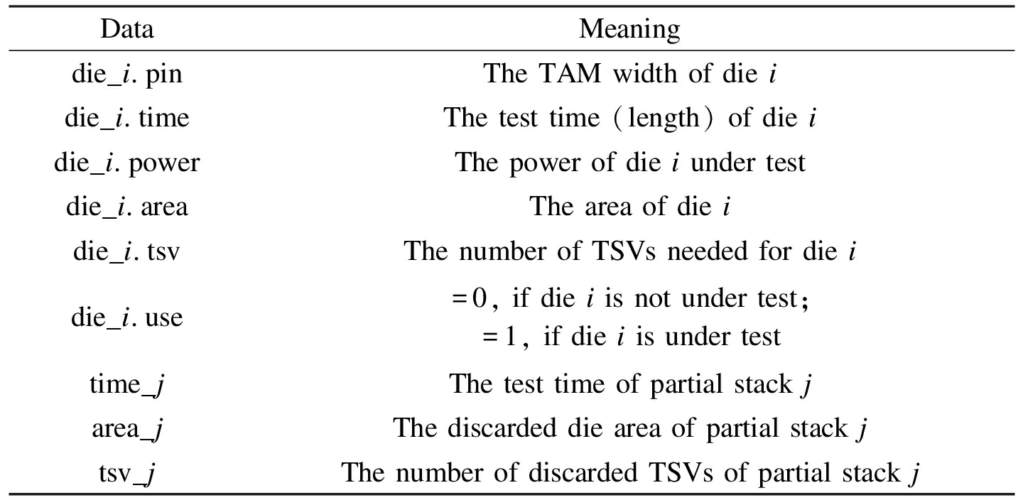
The parameters of each die or each partial stack will be stored in the data type as illustrated in Tab.1. The first 6 parameters reflect the information of each die, and they will be used in Algorithm 1 for test time optimization. The latter 3 parameters, respectively, describe the test time, discarded die area, and the number of discarded TSVs of each partial stack, which will be used in Algorithm 2 for test cost optimization.
3.2 Algorithm 1 for test time optimization in mid-bond testing
Tab.1 The data type for algorithm

DataMeaningdie_i.pinThe TAM width of die idie_i.timeThe test time (length) of die idie_i.powerThe power of die i under testdie_i.areaThe area of die idie_i.tsvThe number of TSVs needed for die idie_i.use=0, if die i is not under test;=1, if die i is under testtime_jThe test time of partial stack jarea_jThe discarded die area of partial stack jtsv_jThe number of discarded TSVs of partial stack j
Algorithm 1 is used to calculate the optimal test time of partial stack PS(j) for mid-bond testing. For a partial stack PS(j) containing j layers, each layer is a die with its parameters including test length, test pin, test power, area and the number of TSVs needed, etc. In addition, the constraints of the maximum test elevators, TAM width and power available are also given. Note that the status of die under test is reflected by the variable die_i.use, which equals 1 when die i is under testing. Moreover, the optimal test schedule for a partial stack will be achieved by optimizing the test time.
Algorithm 1 Test time()
Input: Given a partial stack PS(j) containing j layers, total TAM width available tam_max, upper limit for test power power_max, maximum test elevators between each two layers tsv_max, the parameters of each die;
Output: Optimal test time time_j for partial stack j.
t = 0;
tam = tam_max;
power = power_max;
tsv = tsv_max;
For i:=1 to j Do
if (die_i.pin<=tam && die_i.power && die_i.use=0) Do
tam=tam-die_i.pin;
power=power-die_i.power;
tsv=tsv-die_i.tsv;
die_i.use=1;
if t
t=die_i.time
End if
End if
time_j=time_j+t;
End for
For i:1 to j Do
die_i.use=0;
End for;
Return time_j;
3.3 Algorithm 2 for test cost optimization in mid-bond testing
For a 3D IC containing N layers, there are various combinations of partial stacks. Due to failed bonding, each partial stack may be faulty. If a fault occurs in partial stack PS(j), the latter partial stacks by stacking dies on top of PS(j) will also be faulty and should be discarded, leading to an increase of test cost. In this subsection, we solve the problem of test cost optimization in mid-bond testing. The optimal stacking order can be received by optimizing the test cost. Note that the yield Yps(j) of a partial stack PS(j) can be determined according to the yield modeling in Section 2, and the failed bonding possibility fj for the j-th assembly process is equal to 1-Yps(j).
First, we initialize the parameters of the yield model and cost model according to Section 2. Then, the cost ascending order of dies will be sorted by calculating the test cost of each die. Note that the bottom layer will be tested multiple times, and the latter partial stack testing will contain the testing for Layer 1, thus the lower cost for testing bottom layer means the lower cost for the entail stack. The die with the minimum test cost will be selected as the bottom-most one (Layer 1). After determining Layer 1 (also the partial stack PS(1) in our scheme), the die stacking on top of Layer 1 will be selected by calculating the minimum test cost, and the cost for discarded dies due to failed bonding is considered. Note that Algorithm 1 for test time optimization is called for when calculating the test cost for a partial stack. Then, Layer 2 together with Layer 1 will form partial stack PS(2) with its stack yield Yps(2). Layer 3 is determined by calculating the test cost of PS(3) in each combination and so forth. The test cost calculation is detailed in the pseudo code. Finally, the optimal stacking order is achieved with the minimum test costs.
Algorithm 2 Test cost()
Input: Given a 3D IC containing N layers, failed bonding possibility fj (=1-Yps(j)) for the j-th stacking step, the parameters of each die;
Output: Optimal test cost Cop.
Initialize the parameters of the yield model and cost model; sorting dies in an ascending order of test cost and determine the bottom layer.
For stack j:=1 to N Do
Test time()
For i:=1 to j Do
area_j=die_i.area+fjarea_j;
tsv_j=die_i.tsv+fjtsv_j;
End for
For j:=1 to N Do
T:=T+time_j;
Adie:=Adie+area_j;
NTSV:=NTSV+tsv_j;
End for
Cop =aT+bAdie+cNTSV;
Obtain the optimal stacking order of each layer;
Return Cop;
4 Experiments
In this section, we present the experimental results of the proposed optimal stacking order selection methods for test cost reduction. First of all, the experimental setup is presented. Then, the comparison of proposed stacking order and baselines are given, considering several constraints.
4.1 Experimental setup
We develop our experimental program via C++ and run the benchmarks on a 3.40 GHz Intel i7 processor with 16 GB RAM. All the programs are finished within only a few seconds. In order to demonstrate our optimization scheme, we use ITC’02 benchmark SoCs[9] to realize our experiments as depicted in Tab.2. As most of the benchmark circuits only have the test length information, we assume other information such as area and power. We use the estimation method proposed in Ref.[10]. The area of each core is computed by the summation of input pins, output pins, and scan cells, multiplied by an area density of 3.18×10⁻⁴ mm2/number, which is obtained by the average synthesis results of TSMC 180 nm technology. The test power is computed by the power density of 1.4 mW/mm2, multiplied by the core area.
Tab.2 Parameters for ITC’02 benchmarks

Die numberDie nameTest length /cycleTAM widthDie area/mm2Test power/mW 1d695106 391152.623.662f2126700 665204.966.943p228101 333 098259.2212.914p937912 608 8703030.8243.155p343922 743 317257.3210.24
We assume a defect density of D=0.5 defects/cm2 and a defect clustering parameter α=0.5. Since there is still no concrete model for Ybonding that takes device failure caused by bonding into account and it is typically assumed to be a constant value, then for sake of simplicity, we can assume Ybonding to be 95%[7]. We further assume that there are 1 000 TSVs with 200×10-6 defects implemented in this 3D IC, and then we can obtain the assembly yield of 77.8%[11] in Eq.(2).
Tab.3 Parameters used in proposed test cost model

ParametersValuesf /MHz10CATE /($·s-1)0.23CTSV /($·μm-2)1.4×10-9ATSV/μm210 000Cdie/($·μm-2)4.24×10-8
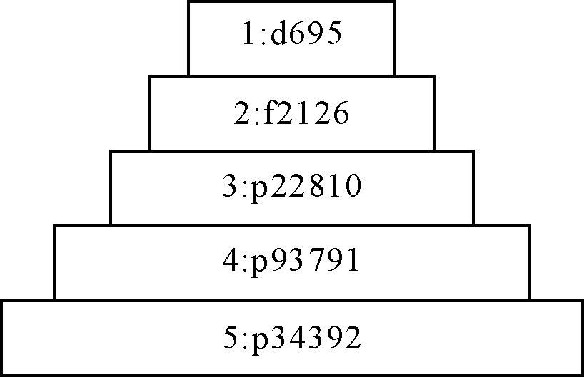
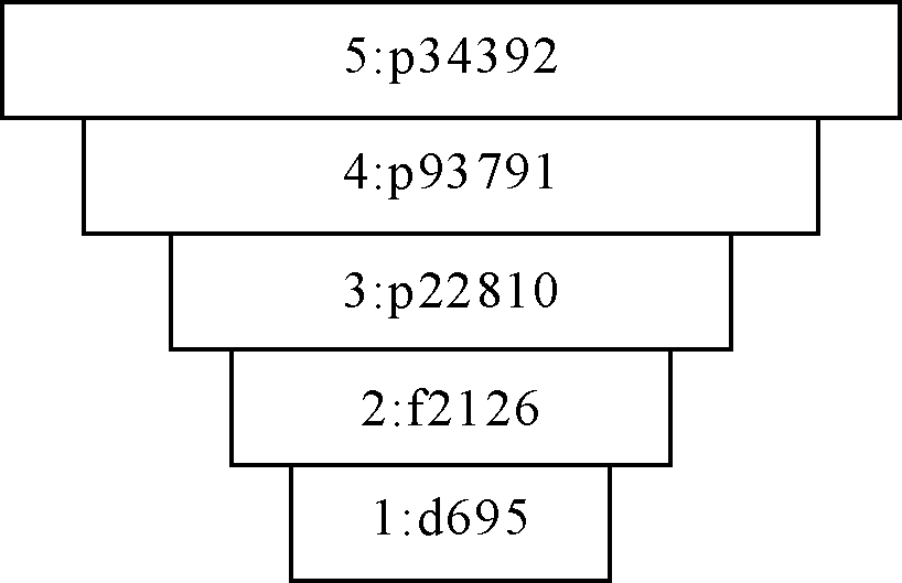
The frequency of the test clock is set to be a typical value of 10 MHz. Tab.3 also lists the parameter values used in our test cost model, which are based on the published data in Refs.[12-13]. The parameter CATE is set to be 0.23 $/s for a typical ATE usage. The parameter Cdie is set to be 4.24×10⁻⁸ $/μm2 and CTSV is set to be 1.4×10⁻⁹$/μm2 for the manufacturing costs. In addition, the parameter ATSV is set to be 10 000 μm2 for a typical TSV pitch of 100 μm.To better prove the effectiveness of our proposed scheme in reducing test cost, we try to run our experiments under various conditions and circuits(see Fig.1). Baseline 1 is in pyramid type with the stacking order in original sequence (die 1 is the bottom layer, namely Layer 1; die 2 is on top of die 1,namely Layer 2, and so forth). Baseline 2 is the reverse order of baseline 1. Then, we will vary the total number of TAM width, test power and the test elevators between each two layers for mid-bond testing. In addition, we will discuss the test cost of our proposed scheme, compared with the baselines. Some substitution words in these tables need to be explained. Baseline means the original stacking order in sequence (die i represents the i-th layer). Proposed represents the optimal stacking order for test cost reduction proposed in this paper. tsv_max, tam_max and power_max represent the maximum test elevators between each two layers, the maximum TAM width and test power available during mid-bond testing. Besides, Ratioi is the reduction percentage of total test costs, which can be obtained as follows:

(a)

(b)
Fig.1 Baselines. (a) Baseline 1 in pyramid type; (b)Baseline 2 in reverse pyramid type
Ratioi = (Baselinei - Proposed)/ Baselinei
(10)
4.2 Impact of TAM width
Tab.4 presents our experimental results of the impact of TAM width on test cost compared with the baseline schemes in sequentially stacking. In order to analyze the impact of TAM width on total test cost, the variable tam_max ,which means the maximum TAM width available, is set to be 35 to 105, the maximum number of test elevators (test TSVs) between each two layers tsv_max is set to be 100, and the maximum test power available power_max is set to be 80. Tab.4 illustrates that compared with baseline 1, our proposed stack reordering scheme can reduce the test costs by around 13.33% at maximum and 12.92% more or less on average. Compared with baseline 2, the optimal order can save test costs by around 65.71% at maximum and 61.66% on average.
4.3 Impact of test TSV
Tab.4 Comparisons between the optimized order and baselines by varying TAM width

ConstraintBaseline 1Baseline 2ProposedRatio/%tsv_maxpower_maxtam_maxOrderCostOrderCostOrderCost1210080351-2-3-4-51.843 765-4-3-2-12.625 391-2-3-5-41.620 5012.1162.0110080451-2-3-4-51.797 875-4-3-2-12.609 271-2-3-5-41.574 6012.4265.7110080551-2-3-4-51.725 765-4-3-2-12.427 941-2-3-5-41.502 5012.9461.5910080651-2-3-4-51.720 875-4-3-2-12.382 481-2-3-5-41.497 6012.9759.0910080751-2-3-4-51.707 205-4-3-2-12.382 481-2-3-5-41.483 9313.0860.5510080851-2-3-4-51.692 655-4-3-2-12.381 161-2-3-5-41.466 9413.3362.3210080951-2-3-4-51.690 215-4-3-2-12.381 161-2-3-5-41.466 9413.2162.32100801051-2-3-4-51.676 545-4-3-2-12.321 161-2-3-5-41.453 2713.3259.72
Tab.5 Comparisons between the optimized order and baselines by varying test TSVs

ConstraintBaseline 1Baseline 2ProposedRatio/%tsv_maxpower_maxtam_maxOrderCostOrderCostOrderCost1250801051-2-3-4-51.769 655-4-3-2-12.547 951-2-3-5-41.531 8413.4466.3360801051-2-3-4-51.720 875-4-3-2-12.411 821-2-3-5-41.497 6012.9761.0570801051-2-3-4-51.720 875-4-3-2-12.411 821-2-3-5-41.483 9313.7762.5380801051-2-3-4-51.692 655-4-3-2-12.351 821-2-3-5-41.469 3913.1960.0590801051-2-3-4-51.690 215-4-3-2-12.381 161-2-3-5-41.466 9413.2162.32100801051-2-3-4-51.676 545-4-3-2-12.321 161-2-3-5-41.453 2713.3259.72
Tab.5 presents our experimental results of the impact of test TSV on testing costs compared with the baseline scheme in sequential stacking. In order to analyze the impact of test TSVs on total test costs, the variable tsv_max, which means the maximum test TSVs between each two layers available, is set to be 50 to 100. The maximum TAM width available tam_max is set to be 105, and the maximum test power available power_max is set to be 80. Tab.5 illustrates that compared with baseline 1, our proposed stack reordering scheme can reduce test costs by around 13.77% at maximum and 13.32% more or less on average. Compared with baseline 2, the optimal order can save the test costs by around 66.33% at maximum and 62% on average.
4.4 Impact of test power
Tab.6 presents our experimental results of the impact of test power on test cost compared with the baseline scheme in sequentially stacking. In order to analyze the impact of test TSVs on total test costs, the variable power_max which means the maximum test power available, the maximum TAM width available tam_max, and the maximum number of test elevators (test TSVs) between every two layers tsv_max are set to be 50 to 80, 105, and 100. Tab.6 illustrates that compared with baseline 1, our proposed stack reordering scheme can reduce test costs by around 14.63% in maximum and 13.71% more or less on average. Compared with baseline 2, the optimal order can save test costs by around 65.55% and 63.09% on average.
Tab.6 Comparisons between the optimized order and baselines by varying test power

ConstraintBaseline 1Baseline 2ProposedRatio/%tsv_maxpower_maxtam_maxOrderCostOrderCostOrderCost12100501051-2-3-4-51.764 765-4-3-2-12.501 171-2-3-5-41.510 8314.3965.55100551051-2-3-4-51.735 415-4-3-2-12.441 171-2-3-5-41.481 4914.6364.78100601051-2-3-4-51.720 875-4-3-2-12.441 171-2-3-5-41.481 4913.9164.78100651051-2-3-4-51.707 205-4-3-2-12.441 171-2-3-5-41.481 4913.2264.78100701051-2-3-4-51.690 215-4-3-2-12.381 161-2-3-5-41.466 9413.2162.32100751051-2-3-4-51.676 545-4-3-2-12.321 161-2-3-5-41.453 2713.3259.72100801051-2-3-4-51.676 545-4-3-2-12.321 161-2-3-5-41.453 2713.3259.72
4.5 Impact of stack size
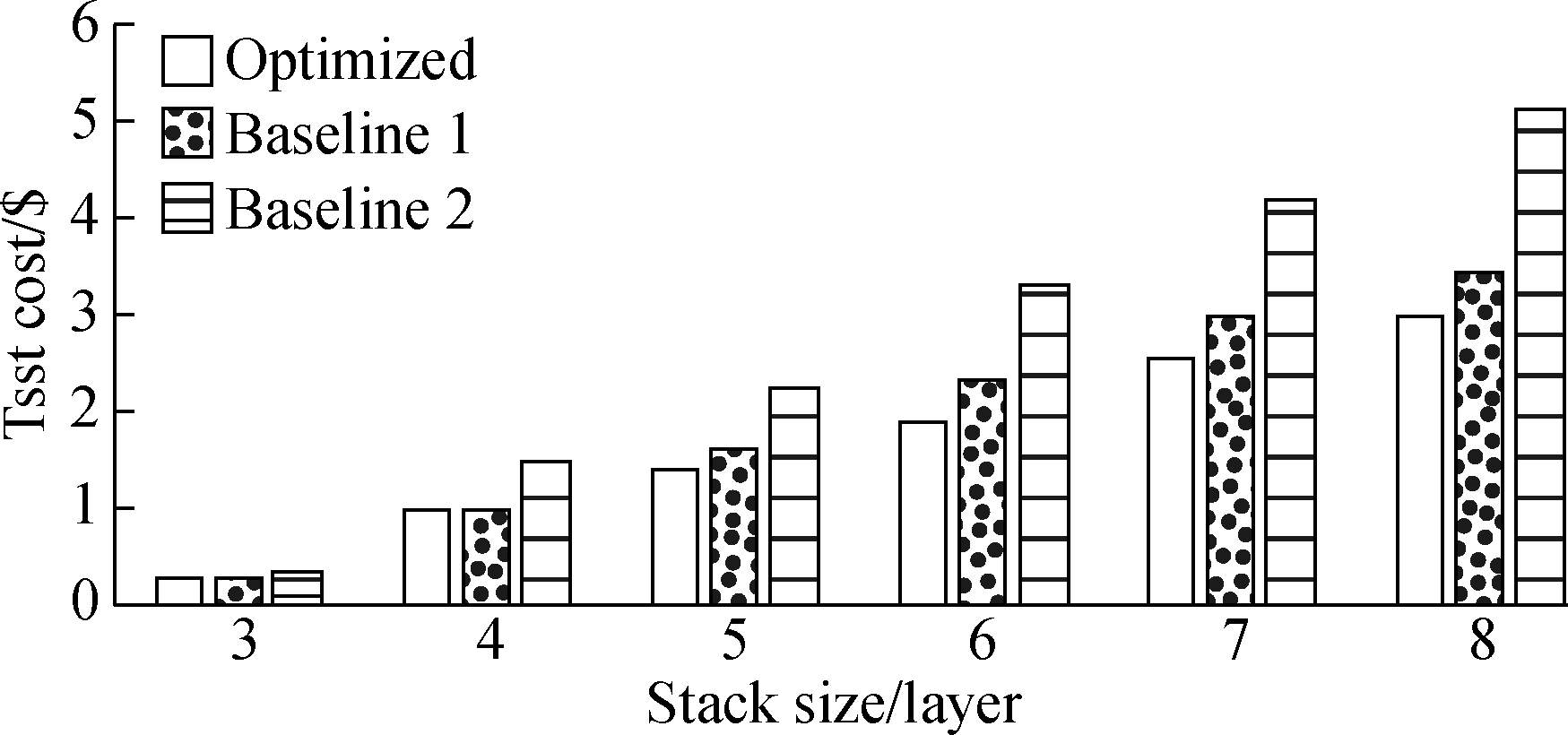
Fig.2 depicts the mid-bond test costs of different stack orders under various stack sizes. We can see that test cost increases as the stack size increases. Furthermore, with the increase of the stack size, the optimized stack order can save much more test cost, which also proves the effectiveness and significance of the proposed stacking order for test cost reduction.

Fig.2 Test costs of different stack orders under various stack sizes
5 Conclusion
In this paper, we propose an optimal stacking order scheme of 3D IC for mid-bond testing to reduce test costs. Due to failed bonding, if one defect occurs in a partial stack, then larger latter partial stacks will be faulty and discarded. In addition, the bottom dies will be tested repeatedly many times, thus the lower cost of testing the bottom dies helps to save the overall test cost during mid-bonding. To prove the effectiveness of the proposed stacking order, we compare two baselines stacked sequentially either in pyramid type or in inverted pyramid type. Based on the benchmarks from ITC’02, experimental results show that for a 5-layer 3D IC, the optimal stacking order can significantly save total test costs. Furthermore, with the increase of the stack size, the optimized stack order can save much more test cost, which also proves the effectiveness and significance of the proposed stacking order on test cost reduction.
[1]Agrawal M, Chakrabarty K. Test-cost modeling and optimal test-flow selection of 3D-stacked ICs [J]. IEEE Transactions on Computer-Aided Design of Integrated Circuits and Systems, 2015, 34(9):1523-1536.
[2]Agrawal M, Chakrabarty K. Test-cost optimization and test-flow selection for 3D-stacked ICs [C]//2013 IEEE 31st VLSI Test Symposium (VTS). Berkeley, CA, USA, 2013:1-6. DOI:10.1109/vts.2013.6548941.
[3]Taouil M, Hamdioui S. Test impact on the overall die-to-wafer 3D stacked IC cost [J]. Journal of Electronic Testing, 2012, 28(1):15-25.
[4]Taouil M, Hamdioui S. Stacking order impact on overall 3D die-to-wafer stacked-IC cost [C]// IEEE International Symposium on Design and Diagnostics of Electronic Circuits & Systems. Cottbus, Germany, 2011:335-340.
[5]Liang H G, Chang H. Optimized mid-bond order for 3D stacked ICs considering failed bonding [J]. Chinese Journal of Electronics, 2015, 24(2):223-228. DOI:10.1049/cje.2015.04.001. (in Chinese)
[6]Koren I, Koren Z. Defect tolerance in VLSI circuits: Techniques and yield analysis [J]. Proceedings of the IEEE, 1998, 86(9):1819-1838. DOI:10.1109/5.705525.
[7]Chen Y,Niu D,Xie Y.Cost-effective integration of three-dimensional ICs emphasizing testing cost analysis [C]// IEEE International Conference on Computer-Aided Design. San Jose, CA, USA, 2010: 471-476.
[8]Deng Y D,Maly W P. 2.5-dimensional VLSI system integration [J]. IEEE Transactions on Very Large Scale Integration Systems, 2005, 13(6):668-677.
[9]Krishnendu C. ITC’02 SOC test benchmarks [EB/OL]. (2008-08-22)[2017-05-20]. http://itc02socbenchm.pratt.duke.edu.
[10]Hsu C Y,Kuo C Y, et al. 3D IC test scheduling using simulated annealing [C]// International Symposium on VLSI Design, Automation, and Test. Hsinchu,China, 2012:1-4.
[11]Jiang L,Xu Q. Yield and reliability enhancement for 3D ICs: Dissertation summary: IEEE TTTC E.J. McCluskey doctoral thesis award competition finalist [C]// IEEE International Test Conference. Anaheim, CA, USA, 2015:1-11. DOI:10.1109/test.2015.7342423.
[12]Cadix L. Lifting the veil on silicon interposer pricing [EB/OL]. (2012-12)[2017-05-20]. http://electroiq.com/blog/articles/2012/12/lifting-the-veil-on-silicon-interposer-pricing/.
[13]Wang R,Chakrabarty K, Bhawmik S. Interconnect testing and test-path scheduling for interposer-based 2.5-D ICs [J]. IEEE Transactions on Computer-Aided Design of Integrated Circuits and Systems, 2015, 34(1):136-149.DOI: 10.1109/TCAD.2014.2365097.