With the development of deep submicron and nanometers technology in VLSI, the reliability evaluation for high level circuits has increasingly become the focus of attention[1]. Furthermore, the circuits in newer VLSI manufacturing technologies are more prone to dynamic errors caused by reduced noise margin, lower supply voltage and a low stored charge in circuit nodes[2]. This makes VLSI become very sensitive to the signal probability (SP) of logic circuits, such as soft (transient) errors and random process variation[3].
However, the complexity of the exact calculation for the signal probability grows exponentially with the circuit size, which is caused by the signal correlations arising from reconvergent fan-outs (RFOs). Therefore, the task of signal probability computation was regarded as a sharp-P-complete problem[4], which is possibly even more difficult than a NP-complete problem.
To deal with the complex problem, several algorithms have been proposed for signal probability computation in search for a good trade-off between accuracy and computational complexity, such as the weighted averaging algorithm (WAA)[5], the improved weighted averaging algorithm (IWAA)[6-7], the probabilistic gate model (PGM)[8-9], probabilistic transfer matrices (PTM)[10-11], Bayesian networks (BN)[12], probabilistic decision diagrams (PDD)[13], and stochastic computational models (SCM)[14]. The several aforementioned algorithms have certain impact, but they are inaccurate or have high computational complexity.
In this paper, a new method based on the IWAA is proposed to calculate the signal probability of logic circuits under multiple independent errors, where a failure in each gate is assumed to affect the output with a probability, i.e., gate error rate, regardless of other gate failures. The steps are as follows: First, calculate the initial signal probability of each lead by a simple logic function that provides a transform of the signal probability from input to output. Secondly, find the reconvergent fan-ins (RFIs) where the fan-out branch is convergent for the first time. Then, calculate the signal probability of RFIs with the weighted average. Finally, introduce some correction terms into the signal probability equation for RFIs to improve the accuracy of the algorithm. Our proposed method is probably suitable for circuits without RFOs. The empirical evidence indicates that our approach improves computational efficiency and its accuracy is acceptable.
1 Background
1.1 Signal probability
The main difficulty of the signal probability computation is the presence of the reconvergent fan-out[5], including the effects of the fan-out branch, multiplicity dependencies and signal correlation, which are the main sources of error. Monte Carlo (MC) simulation is an accurate method recognized by the VLSI community and is often used to simulate circuit behaviors[15]. Therefore, it is applied to calculate the signal probability.
However, large simulations in MC are needed to ensure its accuracy due to its random sampling. The approach of algebraic operations upon probabilities is used to the signal probability computation. It is simple and generic due to the fact that this approach associates variable names with each of the input leads representing the signal probability of the input lead[5] and computing the signal probability of each output lead with algebraic expressions including these variables.
In this paper, we assume that the binary input or output signal of the gate is associated with a variable that denotes the signal probability of the gate. The signal probability is defined as the probability that the signal is a logical “1”, i.e. p (signal = 1)[3].
For convenience, unless otherwise stated, the signal probability of lead A called pA refers to the probability that the logic signal of A is “1” in the following sections.
The formula of the signal probability calculation for the logic gates with two-input and fault-free was proposed in Ref.[16]. For instance, if the signal probabilities of the inputs for AND gate are p1 and p2, the signal probability of the output is p1p2. In the case of the OR gate, the signal probability of the output is equal to 1-(1-p1)(1-p2). In general, the formulas of the signal probability calculation are shown in the Tab.1. For the XOR gate, the simplified formula is complicated due to the multiple input gates, so only gates with two inputs are given.
In fact, any gates in a circuit may fail, namely a von Neumann error, which flips the correct output of a gate and resembles the behavior of a soft error[14]. Therefore, the computation formula of the signal probability sA for the logic gate can be expressed as[8]
sA=pA(1-ε)+(1-pA)ε
(1)
where pA is the output signal probability of lead A with fault-free computed by the rules in Tab.1 and ε is a constant error rate of the gate.
Tab.1 Set of rules for calculating the lead signal probabilities of the logic circuits which are fault-free
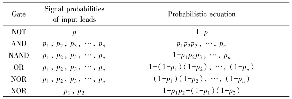
GateSignal probabilities of input leadsProbabilistic equationNOTp1-pANDp1, p2, p3, …, pnp1p2p3, …, pnNANDp1, p2, p3, …, pn1-p1p2p3, …, pnORp1, p2, p3, …, pn1-(1-p1)(1-p2), …, (1-pn)NORp1, p2, p3, …, pn(1-p1)(1-p2), …, (1-pn)XORp1, p21-p1p2 -(1-p1)(1-p2)
Indeed, if a logic circuit is fan-out free, the signal probability can be computed correctly in linear time[3,6], and the calculation process in Ref.[8] is as follows.
Algorithm 1 A signal probability estimation for logic circuits with fan-out free
Input: A logic circuit;
Output:An estimation of the signal probability of each lead in the logic circuit.
Compile the circuit by organizing it into levels.
Assign signal probabilities of 1/2 to all the primary inputs (PIs) and set the value of the error rate of ε.
Compute the signal probability of each lead from the PIs to the primary outputs (POs) in the circuit using the formulas shown in Tab.1 and Eq.(1).
End the algorithm.
We further illustrate Algorithm 1 using a simple circuit as follows. As shown in Fig.1, the circuit has no RFO and the gate error rate ε=0.1. First, the circuit is compiled and partitioned into three levels. Then the signal probabilities of PIs are set to be 0.5, namely, pA=pB=pC=pD=0.5, which are also used in later cases in this paper. Finally, the signal probability of each lead in the circuit can be computed by Algorithm 1. The calculation procedures are as follows: 1) pE=pApB=0.25, sE=pE(1-ε)+(1-pE)ε=0.3; 2) pF=1-(1-pC)(1-pD)=0.75, sF =pF(1-ε)+(1-pF)ε=0.7; 3) pG=sEsF=0.21, sG=pG(1-ε)+(1-pG)ε=0.268.
Particularly, if the logic circuit is fan-out free, Algorithm 1 yields exact signal probabilities. By contrast, Algorithm 1 yields an approximation for the signal probability[2-3]. Hence, Algorithm 1 can be successfully applied to the parts of general circuits that are fan-out free, otherwise it results in an approximate result.
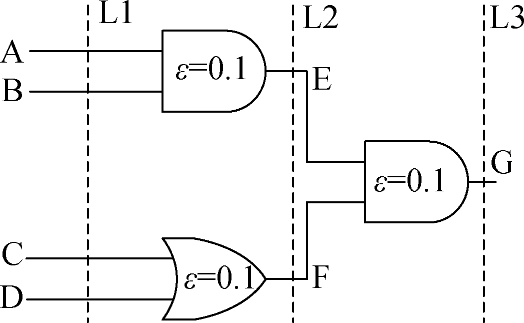
Fig.1 Schematic of a simple circuit
1.2 Basic idea of the IWAA
Ref.[6] proposed the IWAA based on the WAA which overcomes the drawback of the WAA, but it is inaccurate in estimating the effects of RFOs on the circuit, since the WAA uses a weighted average as the value of signal probabilities associated with the PIs.
Given a logic circuit, if lead A is a reconvergent fan-out, then the signal probability computation of Algorithm 1 for lead S beyond that reconvergent node is likely to be erroneous due to the multiple dependencies on A[5]. There is a simple modification of Algorithm 1 to avoid and reduce such error. The signal probability equation is given as[3-4]
SA=SA(0)(1-pA)+SA(1)pA
(2)
where SA is the signal probability of S associated with A; SA(0) and SA(1) are the signal probability of S when the signal probability of A is set to be 0 and 1, respectively.
There is only one RFO in a circuit that is similar to the circuit presented in Fig.1. As shown in Fig.2, SA is equal to 0.268 when it is calculated by Algorithm 1. However, the result of SA is incorrect, caused by the signal correlation of the fan-out branch (A1 and A2). However, the real value of SA is equal to 0.6, which can be computed by Algorithm 2[4,6]. However, for the circuit with multiple RFOs, Algorithm 2 cannot obtain a good calculation precision.
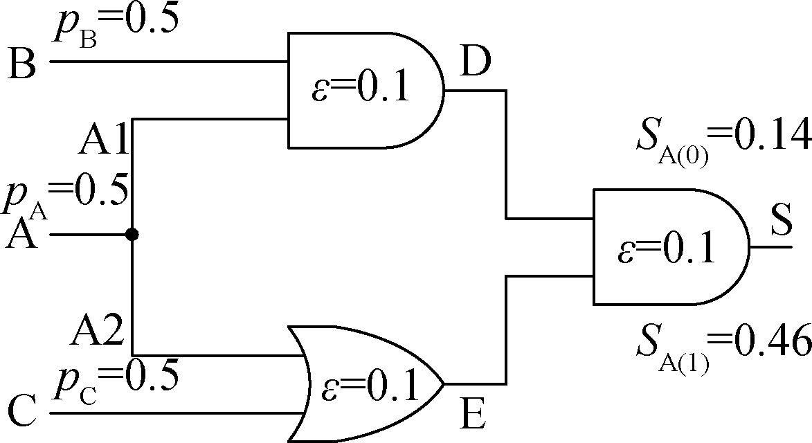
Fig.2 A simple circuit with one RFO
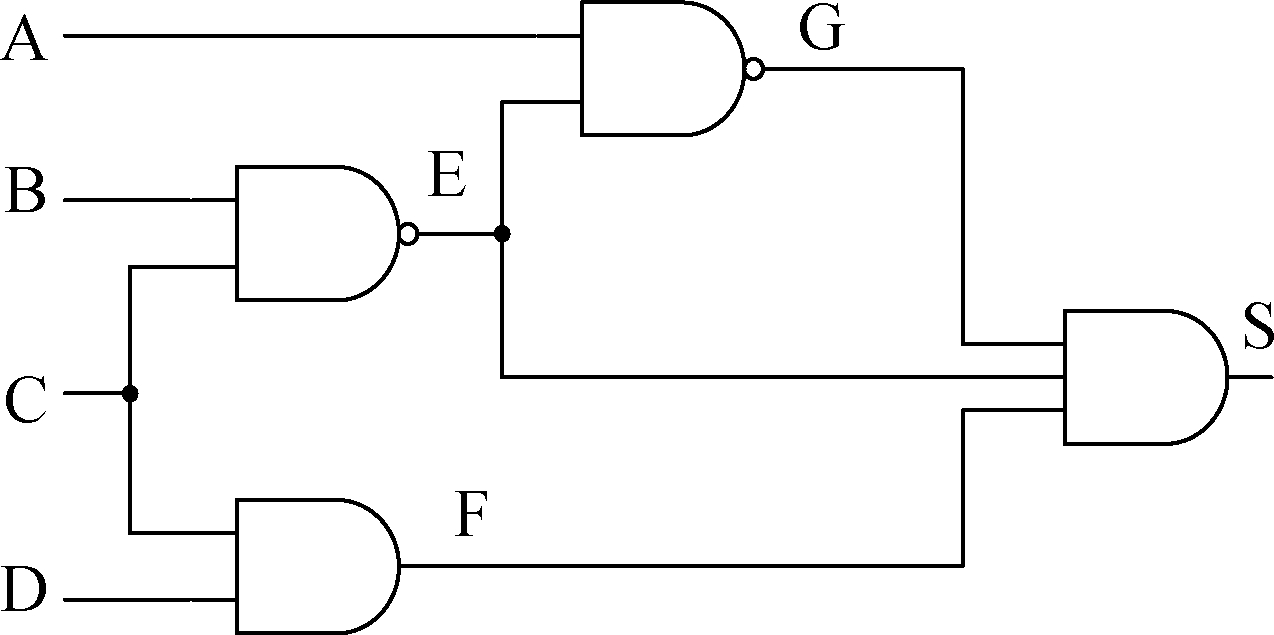
Fig.3 A circuit with two RFOs
Algorithm 2 A signal probability estimation method associated with the reconvergent fan-out
Input: A logic circuit with only one RFO, a reconvergent fan-out A, lead S beyond the reconvergent node;
Output: An estimation of the signal probability of S in the logic circuit.
Calculate the signal probability pA of A by Algorithm 1.
Compute SA(0) and SA(1) from A to S using the formulas shown in Tab.1 and Eq.(1) when the signal probability of A is set to 0 and 1, respectively.
Calculate SA of S using Eq.(2).
End the algorithm.
Ref.[6] defined dependency as a partial order relationship if there is a path from lead C to the POs and lead E in this path, E depending on C (see Fig.3). Furthermore, for lead S, the minimum reconvergent fan-out set (MRFS)[6] of S is a set; i.e., (MRFS(S) is {C}, as shown in Fig.3) where each element, which is reconvergent fan-out, reconverges at S for the first time and does not depend on any other reconvergent fan-outs in the MRFS.
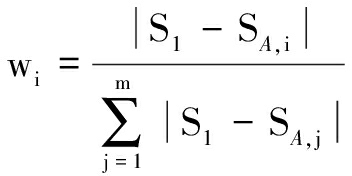
In the IWAA[6], if A1, A2, A3, …, Am are the elements in the MRFS of lead S, the signal probability S of S can be calculated according to the following steps: 1) Compute the signal probability S1 of S by Algorithm 1; 2) Calculate SA,i(1≤i≤m) by Algorithm 2; 3) Compute the weighted average estimate S of the signal probability of lead S by the following formula[6].

(3)
where
(4)
In view of the above-mentioned discussion, finding the MRFS of lead S is the crucial part. The importance of finding the MRFS(S) is to find the minimum reconvergent fan-out from these RFOs which are between PIs and S.
To a certain extent, the IWAA improves the precision of the signal probability estimation. It calculates the signal probability of lead S by the weighted average method associated with elements of MRFS(S). However, it only considers the effects of the reconvergent fan-outs in the MRFS and obtains the corrected signal probability of S. However, it does not consider the effects of some interesting RFOs. Taking Fig.3 as an example, the IWAA estimates the signal probability of lead S without considering the reconvergent fan-out E. Furthermore, it does not consider the effects of the reconvergent fan-ins which are in the paths from elements of MRFS(S) to S. For example, the IWAA estimates the signal probability of lead L (see Fig.5) without considering the impact of the reconvergent fan-in H.
Hence, an improved method based on the IWAA[6] is proposed in this paper to improve its computational accuracy and reduce time complexity.
2 Structure of Reconvergent Fan-Out
The main problem of signal probability calculation for logic circuits is the need to consider the mutual effects of RFOs, since the gate inputs are correlated at the reconvergent nodes. Furthermore, there is more than one RFO in generic, so the correlations of the inputs of reconvergent fan-ins are complex. For ease of understanding, in this section, we introduce some concepts about the basic structures of RFO.
2.1 Single structure with reconvergent fan-out
The single structure with reconvergent fan-out consists of one RFI and one RFO corresponding to the RFI. It can be divided into completely independent reconvergent fan-out and half embedded reconvergent fan-out, according to the relationship between reconvergent fan-outs and reconvergent fan-ins.
There is a single structure with reconvergent fan-out of the circuit, as shown in Fig.4. It is B→F with the structure of completely independent reconvergent fan-out. In this structure, there is no other reconvergent fan-ins in the path from reconvergent fan-out B to reconvergent fan-in F.
In Fig.5, there are two structures of univocal reconvergent fan-out. B→H is the structure of completely independent reconvergent fan-out and C→L is the structure of half embedded reconvergent fan-out. H is a reconvergent fan-in in the structures of B→H and C→L. However, the reconvergent fan-out of B, which is part of the structure of B→H, is not in the path of C→L.
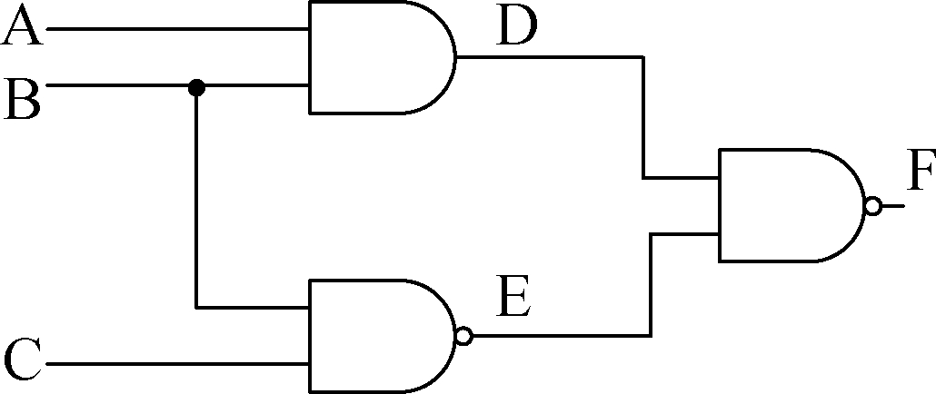
Fig.4 Structure of completely independent reconvergent fan-out
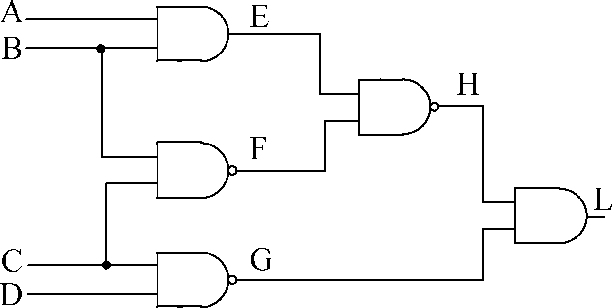
Fig.5 Structure of half embedded reconvergent fan-out
2.2 Multiple structure with reconvergent fan-out
For the circuit that contains two or more structures with reconvergent fan-out, they can be divided into the independent, parallel and embedded types[17] by the relationship between the structures with reconvergent fan-out.
The structures of B→G and C→H are completely independent reconvergent fan-out (see Fig.6), and they have no common nodes.

Fig.6 Structure of independent reconvergent fan-out
The structure of parallel reconvergent fan-out has two or more structures with the same RFI. For example, in the structures of A→E and B→E (see Fig.7), they have some common nodes and the same RFI E.
The structure of the embedded structure is that other single structures are included in the structure. As shown in Fig.8, E→H is the structure of completely independent reconvergent fan-out and it is contained in the structure of C→I.
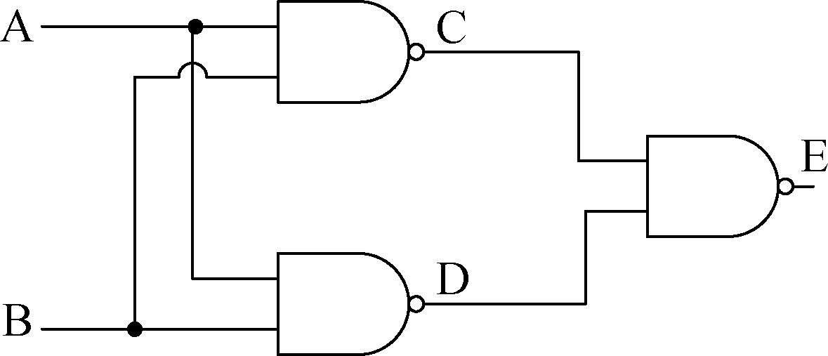
Fig.7 Structure of parallel reconvergent fan-out
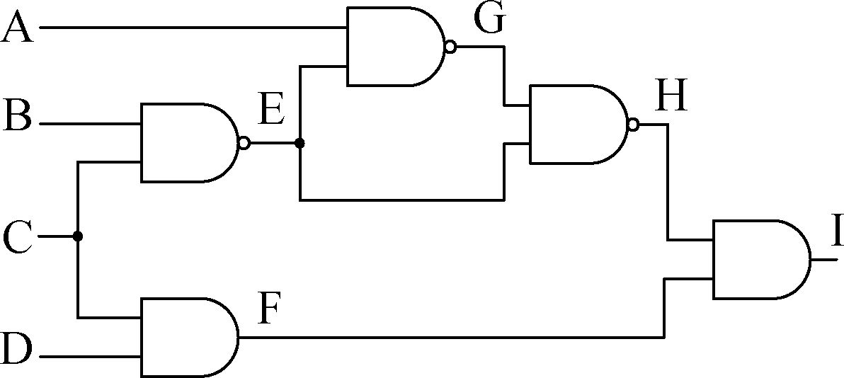
Fig.8 Structure of embedded reconvergent fan-out
3 Signal Probability Calculation
For a simple circuit with a structure of embedded reconvergent fan-out, it will be straightforward for us to iteratively calculate the accurate signal probability of each lead in the circuit by Algorithm 2. However, the actual circuit contains many structures of reconvergent fan-out and its scale is very large, so it requires high time and space complexity to compute the signal probability by using this approach.
In this paper, we present a concept of the nearest reconvergent fan-out set (NRFS): the NRFS(S) is a RFO set of lead S called FRFI which is RFI in the logic circuit, and each element in the set is RFO and converges at S for the first time. For example, the NRFS(S) is {C, E} (see Fig.3). Compared with MRFS, NRFS does not consider the dependencies between elements in the set.
3.1 A weighted average method
It is not acceptable to consider the influence of each structure of reconvergent fan-out as a whole and calculate the signal probability of each gate of the logic circuit.
We propose a weighted average algorithm based on NRFS for the signal probability calculation. In our proposed approach, the signal probability of the reconvergent fan-in is estimated by considering the effect of recent several RFOs, namely the NRFS of the RFI. The proposed method, developed to implement the idea as indicated earlier in this paper, consists of the following main details.
Algorithm 3 The weighted average algorithm with the reconvergent fan-in
Input:A logic circuit;
Output:An estimation of the signal probability of each lead in the logic circuit.
Step 1 Parse circuit and initialize the related parameters.
1.1 Compile the circuit and organize it into levels. Then determine the order in which the leads of the circuit are to be processed.
1.2 Assign signal probabilities of 1/2 to all the PIs and set the value of gate error rate ε. Add the RFO to the reconvergent fan-out set, namely RFOS, at once.
Step 2 Find the FRFI of each RFO of RFOS, and mark the FRFI, then add this RFO to the NRFS of the FRFI.
Step 3 Compute the SP for each lead from the PIs to the POs in the circuit.
3.1 Traverse the circuit, if it reaches the end of the circuit, then go to step 4; else go to 3.2;
3.2 Extract the i-th lead (denoted as gi) from the circuit, if gi is FRFI, then go to 3.4; else go to 3.3;
3.3 Compute the SP of gi using the formulas in Tab.1 and Eq.(1), then go to 3.6;
3.4 For each element of NRFS of gi(Ai,1, Ai,2, Ai,3, …, Ai,m), calculate the relative signal probability SAi,j(1≤j≤m) with Algorithm 2;
3.5 Compute the weighted average signal probability Sw,i of gi with Eqs. (3) and (4), then make the SP of gi equal Sw,i;
3.6 Perform i=i+1 and go to 3.1.
Step 4 End the algorithm.
From the above, the circuit is traversed once in Step 1 of Algorithm 3, then the basic information (lead) of the logic circuit is extracted and the related parameters are initialized. Therefore, the time complexity of Step 1 can be O(L). In Step 1, the main information that needs to be stored is the lead information of the circuit, the information of the RFOs and other intermediate variables, so that the space complexity of Step 1 is O(L+FO+c). For each RFO, the circuit is traversed from the location of the RFO and the FRFI of the RFO in Step 2 is found, so the time complexity is less than or equal to O(LFO). In addition, in the process of computing, for each of the FRFI needs, the information of its corresponding RFOs is stored. Therefore, the space complexity of Step 2 is O(FO). Step 3 is the signal probability calculation of the lead. For the FRFI, the lead, which is in the path from the NRFS of the FRFI to the FRFI, is calculated twice. For other leads, the SP can be computed by Eq.(1) and the formulas in Tab.1. Therefore, the time complexity of Step 3 is less than or equal to O(2LFO+L-FI). In the analysis, the total time-space complexity of Algorithm 3 is less than or equal to O((3FO+2)L-FI) and O(gn+2FO+c), respectively, where L is the number of leads; FO is the number of RFOs; FI is the number of FRFIs; and c is a constant. In other words, from PIs to POs, Algorithm 3 is always calculated in each lead in units of basic gates. In addition, since FI and FO are far smaller than L, the time and space complexities of Algorithm 3 have approximate linear growth with the number of leads.
In Algorithm 3, it is a critical step to make sure that the FRFI can be found quickly and accurately. Therefore, we select one RFO that is only selected once and find the corresponding FRFI. In order to illustrate the process, we take the circuit of Fig.6 as an example. First, identify the RFOs (B, C) while compiling the circuit. Then, find the corresponding FRFI from these RFOs, and G is the FRFI of B and H is the FRFI of C. Finally, correct the SP of the lead which depends on RFIs. Therefore, we should quickly mark the positions of the RFOs and the corresponding FRFI before correcting the signal probability. It will avoid unnecessary computation and improve the efficiency of execution.
Nevertheless, for each lead which depends on RFOs (such as E, F, G and H in Fig.6), the IWAA will execute this step of finding the MRFS while the SP of this lead is calculated. Compared with the IWAA, Algorithm 3 avoids repeated judgment and greatly reduces the processing time.
3.2 A strategy correction method
Moreover, there are some distinct deviations in the signal probability calculation of the FRFIs using Algorithm 3. The reason is that there is a correlation between the input signals of FRFIs. Therefore, for each RFI in a circuit, we should correct these inaccuracies in addition to using the weighted average approach.
Nevertheless, during signal transmission, the signal of fan-out branches from the same RFOs may constantly converge or branch which results in the signal correlation accumulation and increases the computing complexity. Besides, for lead S, not only the effect of the RFOs in the NRFS of S but also that of the input signals of S is crucial. Also, other RFOs on which S depends have certain impact on the signal probability of S.
Therefore, the estimated value obtained by the weighted average approach is still imprecise and should be corrected, if there are other FRFIs in the path from the FRFI to its corresponding NRFS, such as the two examples shown in Fig.5 and Fig.6; or if the correlation of the input signals of the RFI is complex, such as the example shown in Fig.5. Some correction terms are introduced into the equation based on the weighted average approach.
The signal probability of lead S estimation formula is as follows:
(5)
where
(6)
(7)
where Su is the estimated signal probability; ![]() is a weighted average of Sw and S1. For the signal probabilities Sw, S1 and si (si is the initial signal probability without considering the effect of RFOs), in most cases, Sw has the highest accuracy, so Su=Sw. However, in the case of |Sw-S1|≤0.1Sw, that is
is a weighted average of Sw and S1. For the signal probabilities Sw, S1 and si (si is the initial signal probability without considering the effect of RFOs), in most cases, Sw has the highest accuracy, so Su=Sw. However, in the case of |Sw-S1|≤0.1Sw, that is ![]() β is the correction term which can make a few modifications to the influence from NRFS and the correlation of the input signal of S; ∂ is the symbol item, of which the value is 0, 1 or -1; s′ is the product of the signal probability of the elements in NRFS of S; smin is the minimum element of a set which is made up of the input signal probabilities of S and the absolute values for the difference between the input signal probabilities and 1; sα is one of signal probabilities of all input signals or the average value of signal probabilities of some input signals. Furthermore, the selection principle of input signals is to minimize parameter θ(θ=|1-s′/sS|).
β is the correction term which can make a few modifications to the influence from NRFS and the correlation of the input signal of S; ∂ is the symbol item, of which the value is 0, 1 or -1; s′ is the product of the signal probability of the elements in NRFS of S; smin is the minimum element of a set which is made up of the input signal probabilities of S and the absolute values for the difference between the input signal probabilities and 1; sα is one of signal probabilities of all input signals or the average value of signal probabilities of some input signals. Furthermore, the selection principle of input signals is to minimize parameter θ(θ=|1-s′/sS|).
As shown in Tab.2, the value of ∂ is determined by S1, Sw and s. If S1+Sw-2s′>0, the exact signal probability of S is likely to be higher than the three signal probabilities, so we can slightly modify Su and make it larger. When S1+Sw-2s′<0, we do the opposite of what we do for Su. However, if S1+Sw-2s=0, we cannot determine the relationship between the exact signal probability and the three signal probabilities, so we do not carry out any modification for Su.
Tab.2 Values of ∂ for the difference among S1, Sw and s′ of FRFI

S1+Sw-2s′Value of ∂>01<0-1=00
Since the signal probability of FRFIs may be affected by other FRFIs compared with Algorithm 3, we introduce some correction terms into the weighted average equation of Algorithm 3. The algorithm of the strategic correction method for signal probability estimation based on Algorithm 3 is given below.
Algorithm 4 The hybrid strategy combined with circuit structure for signal probability estimation
Input: A logic circuit;
Output: An estimation of the signal probability of each lead in the logic circuit.
Step 1 Perform Steps 1 and 2 of Algorithm 3.
Step 2 Calculate the initial signal probability si of each lead by performing Step 3 of Algorithm 1.
Step 3 Compute the SP for each lead from the PIs to the POs in the circuit.
3.1 Traverse the circuit, if it reaches the end of the circuit, then go to Step 4; otherwise go to 3.2;
3.2 Extract the i-th lead (denoted as gi) from the circuit, then calculate the probability S1 of gi with the formulas in Tab.1 and Eq.(1), then make the SP of gi equal S1;
3.3 If gi is FRFI, then go to 3.4; otherwise go to 3.5;
3.4 Recalculate the SP of gi;
3.4.1 For each element of NRFS of gi (Ai,1, Ai,2, Ai,3, …, Ai,m), calculate the relative signal probability SAi,j (1≤j≤m) using Algorithm 2. If there are other RFIs between the RFOs of NRFS of gi and gi, then mark gi;
3.4.2 Compute the weighted average signal probability Sw,i of gi with Eqs.(3) and (4);
3.4.3 If gi is marked, then go to 3.4.4; otherwise make the SP of gi equal Sw,i, then go to 3.5;
3.4.4 Compute the signal probability sgi of gi with Eqs. (5) to (7), then make the SP of gi equal sgi.
3.5 Perform i=i+1 and go to 3.1.
Step 4 End the algorithm.
As seen from the above, Step 1 of Algorithm 4 is the Steps 1 and 2 of Algorithm 3. Therefore, the time and space complexities of Step 1 are less than or equal to O(LFO+L) and O(L+2FO+c), respectively. Step 2 is the initial signal probability calculation of the lead. Therefore, the time and space complexities of Step 2 are O(L) and O(1), respectively. Step 3 is the signal probability recalculation of the lead. The SP of each lead is computed again by Eq.(1) and the formulas in Tab.1. For some FRFIs, Algorithm 4 calculates the signal probability based on the weighted average signal probability. Therefore, the time complexity of Step 3 is less than or equal to O(2LFO+L+FI). In addition, there is some information about other RFIs for some RFIFs, so the space complexity of Step 3 is less than or equal to ![]() In the analysis, the total time-space complexity of Algorithm 4 is less than or equal to O((3FO+4)L+FI) and less than or equal to
In the analysis, the total time-space complexity of Algorithm 4 is less than or equal to O((3FO+4)L+FI) and less than or equal to ![]() respectively. Therefore, the time and space complexities of Algorithm 4 are slightly larger than those of Algorithm 3.
respectively. Therefore, the time and space complexities of Algorithm 4 are slightly larger than those of Algorithm 3.
4 Simulation Results
To verify the effectiveness and applicability of the proposed method, in a computer with Windows Server 2012 Standard system, 2.3 GHz Intel Xeon E312xx (Sandy Bridge) and 8 GB of RAM memory, we chose some ISCAS85 benchmark circuits for the experiment. All the gates are assumed to have the same gate error rate ε and gates fail each other independently.
First, by comparing with the IWAA[6], the effectiveness of the algorithms proposed in this paper is tested when the gate error rate ε=0, and the results are shown in Tab.3. Then, experiments are performed on Algorithms 3 and 4 for different values of ε. The comparison results of the IWAA[7] are shown in Tab.4. Furthermore, considering that the IWAA[6] can also be used to calculate the SP for the circuit with a gate error rate by using Eq.(1), we conduct some experiments based on Algorithm 3, Algorithm 4 and the IWAA[6], respectively. Simulation results are shown in Figs.9 and 10.
In these experiments, the signal probability of the PIs is 0.5. And each fan-out branch is treated as a gate and has the same gate error rate as other gates. In order to measure the quality of our results, we adopt the mean percentage error (MPE) as the standard.
For the MC, faults are injected into the circuit in pseudo-random mode and the approximation of the signal probability is obtained by counting the ratio of the output signal which is logical “1”. However, for the larger circuit, the time consumption of the MC method with exhaustive failure injection will be difficult to accept. Furthermore, in a small circuit, the loss of precision for the MC is larger[18]. Therefore, in order to obtain a good experimental reference object, for the small-scale circuit of c17, the MC simulation runs more than 107 times. For other benchmark circuits, the times of MC simulation is 106.
Tab.3 shows the evaluation results for some ISCAS85 benchmark circuits with the gate error rate ε=0. The first column is the circuit name, the second column gives the MPE of signal probabilities of POs in our proposed two algorithms (Algorithms 3 and 4) and the IWAA[6]. Tab.4 shows the simulation results of Algorithm 3, Algorithm 4 and the IWAA[7] with different ε used for comparison.
Tab.3 Comparison of the results obtained by different methods (ε=0)
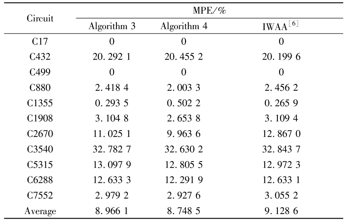
CircuitMPE/%Algorithm 3Algorithm 4IWAA[6]C17000C43220.292 120.455 220.199 6C499000C8802.418 42.003 32.456 2C13550.293 50.502 20.265 9C19083.104 82.653 83.109 4C267011.025 19.963 612.867 0C354032.782 732.630 232.843 7C531513.097 912.805 512.972 3C628812.633 312.291 912.633 1C75522.979 22.927 63.055 2Average8.966 18.748 59.128 6
Tab.4 Comparison of the MPE obtained from Algorithm 3, Algorithm 4 and IWAA[7] for different ε

Circuitε = 0.001ε = 0.01ε = 0.1Algorithm 3Algorithm 4IWAA[7]Algorithm 3Algorithm 4IWAA[7]Algorithm 3Algorithm 4IWAA[7]C499005.30025.00026.69C13554.351.084.51.635.5222.32.622.6526.50C19082.972.541.42.462.178.61.170.999.38C267012.5711.950.96.175.916.00.740.7511.45C354031.8531.682.227.0127.0016.13.695.1518.97Average10.349.452.97.458.1215.61.641.9118.60

(a) (b) (c)
![]()
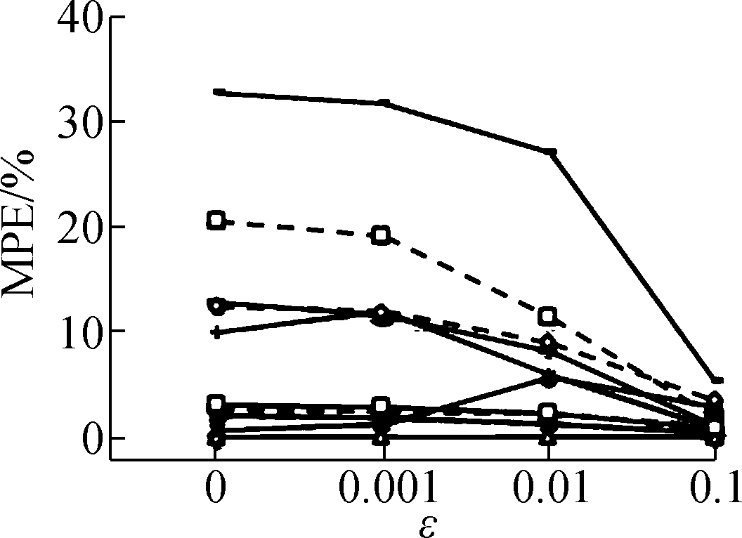
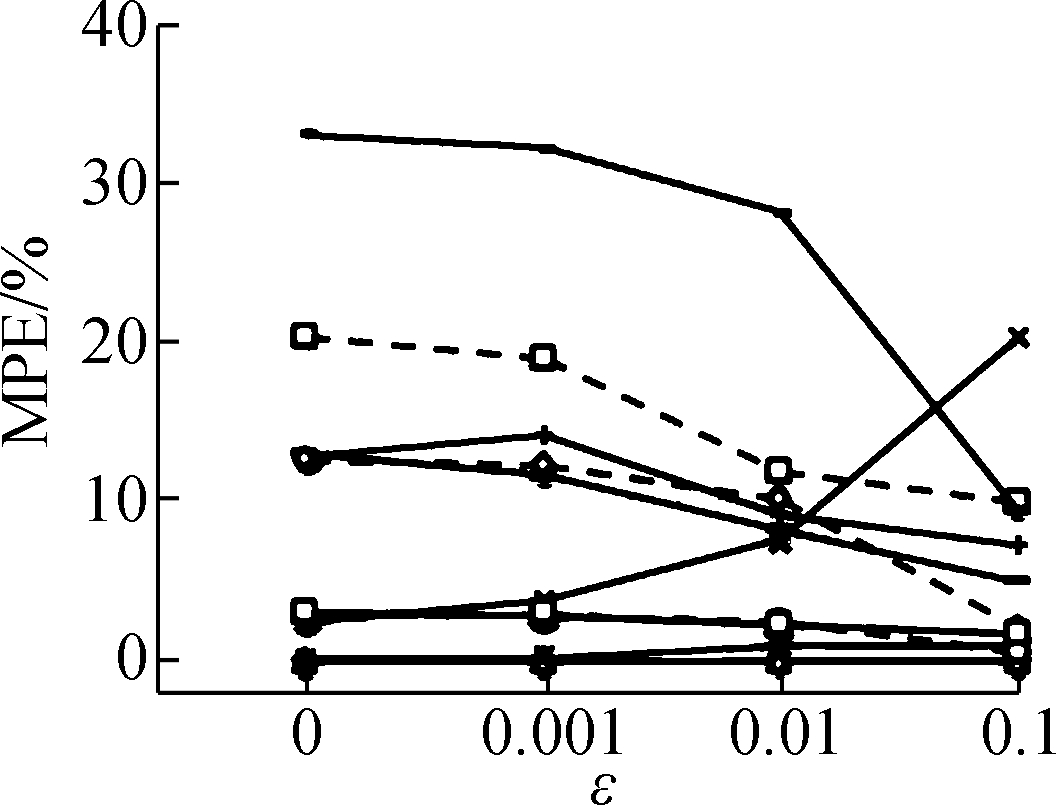
Fig.9 MPE vs. gate error ε . (a) For Algorithm 3; (b) For Algorithm 4; (c) For the novel IWAA

Fig.10 Sum of MPE vs. gate error ε for ISCAS85 benchmarks
Tab.3 reveals that Algorithm 3 and Algorithm 4 have higher accuracy than the approach of IWAA[6] in general. For the MPE, Algorithm 3 has 1.8% improvement and Algorithm 4 has 4.2% improvement relative to the IWWA[6]. In Tab.4, Algorithm 3 and Algorithm 4 are more accurate than the IWWA[7] when the gate error rate ε is greater than 0.01. It demonstrates that when taking the effect of the NRFS of Algorithm 3 and using the mixed-calculation strategy of Algorithm 4, the accuracy of the proposed approaches is improved when ε<0.01.
However, the MPE of C432 and C3540 for these three approaches are higher in Tab.3, which may be caused by the structure of the circuit. The simulation results of C17 and C499 indicate that the proposed approach can calculate the exact signal probabilities for the circuit with fan-out free or with the coupling relationship of RFOs.
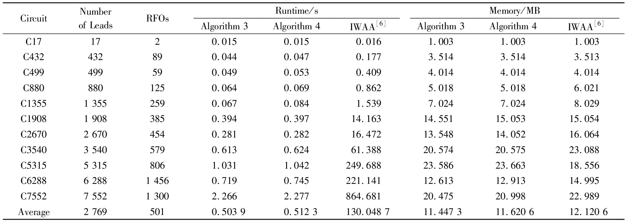
Tab.5 shows the runtime and the memory requirement of the proposed approaches and the IWAA[6] for the ISCAS85 benchmark circuits with 50 experiments and a gate error rate ε = 0. The first column is the circuit name, the second column is the number of leads in the circuit, the third column is the number of RFOs in the circuit, and the fourth column gives the average cost of different methods. Since the IWAA[7] is based on the correlation coefficient method (CCM)[4] and has higher computational complexity than the IWAA in Ref.[6], the runtime and the memory requirement of the IWAA in Ref.[7] are not given to compare with this proposed approach.
Tab.5 reveals that the runtime of Algorithm 3 and Algorithm 4 are much shorter than the IWAA[6], which indicates that our proposed approaches have significant advantages in dealing with large circuits. In most circuits, compared with the IWAA[6], the memory overhead of our approaches are smaller. Previous simulation results indicate that the average speed of our proposed methods is 256× faster than the IWAA[6] and their memory requirements are smaller. The mean accuracy of Algorithm 4 is improved to a certain extent compared with the IWAA[6-7].
In the IWAA[6], the signal probability calculation does not take into account the gate error rate. Therefore, if the circuit is not fault-free, the signal probability can be calculated by the novel IWAA which is based on the IWAA proposed in Ref. [6] and considers the signal probability of the gate calculated by Eq.(1). In order to verify the applicability of the proposed approaches, we conduct the experiment using the novel IWAA and the proposed approaches under the gate error rate of 0.001, 0.01 and 0.1, respectively. The simulation results are shown in Fig.9 and 10.
Tab.5 Comparison of the average time and space consumptions for different methods (ε = 0)
CircuitNumber of LeadsRFOsRuntime/sMemory/MBAlgorithm 3Algorithm 4IWAA[6]Algorithm 3Algorithm 4IWAA[6]C171720.0150.0150.0161.0031.0031.003C432432890.0440.0470.1773.5143.5143.513C499499590.0490.0530.4094.0144.0144.014C8808801250.0640.0690.8625.0185.0186.021C13551 3552590.0670.0841.5397.0247.0248.029C19081 9083850.3940.39714.16314.55115.05315.054C26702 6704540.2810.28216.47213.54814.05216.064C35403 5405790.6130.62461.38820.57420.57523.088C53155 3158061.0311.042249.68823.58623.66318.556C62886 2881 4560.7190.745221.14112.61312.91314.995C75527 5521 3002.2662.277864.68120.47520.99822.989Average2 7695010.503 90.512 3130.048 711.447 311.620 612.120 6
Fig.9 shows the MPE vs. gate error ε for the ISCAS85 benchmark circuits using our proposed approaches and the new IWAA. For the circuits of C17 and C499, these approaches can accurately calculate the signal probability of each lead. Furthermore, such approaches can also be successfully applied to the parts of general circuits that are fan-out free or only have the structures of reconvergent fan-out that are completely independent or independent types. Moreover, the accuracies of Algorithm 3 and Algorithm 4 are much better than that of the novel IWAA when the gate error ε = 0.1.
Fig.10 compares the sum of MPE for ISCAS85 benchmarks, where a smaller error is observed as the gate error rate ε increases. Moreover, in contrast to the novel IWAA, the results of our proposed methods are better. Therefore, our proposed methods have better applicability. When gate error rate ε is from 0 to 0.01, the results evaluated by Algorithm 4 are the best on the whole.
5 Conclusion
A novel approach based on the IWAA is proposed to calculate the signal probability of the logic circuit. The signal probability for each lead in the circuit is calculated by using a weighted averaging method which attempts to take into account the effect of the NRFS and the gate error rate. In addition, some correction terms are introduced into the weighted averaging equation in order to reduce the influence of the signal correlation. The goals of good scalability, low memory requirements and high computational speed are achieved in the proposed method.
The simulation results reveal that the proposed method has approximate linear time computational complexity in terms of the circuit size and the number of RFOs, and its accuracy is higher than that of the IWAA. Theoretical analysis and experimental results demonstrate that our proposed approach is advantageous in terms of efficiency and is easy to implement.
[1]Xiao J, Lou J G, Jiang J H, et al. Blockchain architecture reliability-based measurement for circuit unit importance [J]. IEEE Access, 2018, 6(4): 15326-15334. DOI:10.1109/access.2018.2800712.
[2]Vaghef V H, Peiravi A. A graph based approach for reliability analysis of nano-scale VLSI logic circuits[J].Microelectronics Reliability, 2014, 54(6/7):1299-1306. DOI:10.1016/j.microrel.2014.01.017.
[3]Yu C C, Hayes J P. Scalable and accurate estimation of probabilistic behavior in sequential circuits[C]// 2010 28th IEEE VLSI Test Symposium. Santa Cruz, CA, USA, 2010: 165-170. DOI:10.1109/vts.2010.5469586.
[4]Ercolani S, Favalli M, Damiani M, et al. Estimate of signal probability in combinational logic networks[C]// 1989 1st European Test Conference. Paris, France, 1989: 132-138. DOI:10.1109/etc.1989.36234.
[5]Krishnamurthy B, Tollis I G. Improved techniques for estimating signal probabilities[J].IEEE Transactions on Computers, 1989, 38(7): 1041-1045. DOI:10.1109/12.30854.
[6]Fan Y, Xiang D, Wei D Z. A new signal probability calculation method[J].Microelectronics & Computer, 1995(1): 8-10. (in Chinese)
[7]Choudhury M R, Mohanram K. Reliability analysis of logic circuits[J].IEEE Transactions on Computer-Aided Design of Integrated Circuits and Systems, 2009, 28(3): 392-405. DOI:10.1109/tcad.2009.2012530.
[8]Han J, Chen H, Boykin E, et al. Reliability evaluation of logic circuits using probabilistic gate models[J].Microelectronics Reliability, 2011, 51(2): 468-476. DOI:10.1016/j.microrel.2010.07.154.
[9]Cai S. An efficient reliability estimation method for gate-level circuit[J].Journal of Electronics & Information Technology, 2014, 35(5): 1262-1266. DOI:10.3724/sp.j.1146.2012.01169.
[10]Zandevakili H, Mahani A, Saneei M. An accurate and fast reliability analysis method for logic circuits[J].COMPEL— The International Journal for Computation and Mathematics in Electrical and Electronic Engineering, 2015, 34(3): 979-995.
[11]Xiao J, Lee W, Jiang J, et al. Circuit reliability estimation based on an iterative PTM model with hybrid coding[J].Microelectronics Journal, 2016, 52: 117-123. DOI:10.1016/j.mejo.2016.03.013.
[12]Rejimon T, Lingasubramanian K, Bhanja S. Probabilistic error modeling for nano-domain logic circuits[J]. IEEE Transactions on Very Large Scale Integration Systems, 2009, 17(1): 55-65. DOI:10.1109/tvlsi.2008.2003167.
[13]Abdollahi A. Probabilistic decision diagrams for exact probabilistic analysis[C]// IEEE/ACM International Conference on Computer-Aided Design. San Jose, CA, USA, 2007: 266-272.
[14]Han J, Chen H, Liang J, et al. A stochastic computational approach for accurate and efficient reliability evaluation[J].IEEE Transactions on Computers, 2014, 63(6):1336-1350. DOI:10.1109/tc.2012.276.
[15]Ibrahim W, Shousha M, Chinneck J W. Accurate and efficient estimation of logic circuits reliability bounds[J].IEEE Transactions on Computers, 2015, 64(5): 1217-1229. DOI:10.1109/tc.2014.2315633.
[16]Vaghef V H, Peiravi A. Node-to-node error sensitivity analysis using a graph based approach for VLSI logic circuits[J].Microelectronics Reliability, 2014, 55(1): 264-271. DOI:10.1016/j.microrel.2014.09.010.
[17]Taylor E, Han J, Fortes J. Towards accurate and efficient reliability modeling of nanoelectronic circuits[C]//2006 Sixth IEEE Conference on Nanotechnology (IEEE-NANO). Cincinnati, OH, USA, 2006: 395-398.
[18]Xiao J, Lee W, Jiang J H, et al. Sensitivity evaluation of input vectors with masking effects in digital circuits [J]. Chinese Journal of Computers, 2017, 40(38): 1-14. (in Chinese)