The soft error is of transient error resulting from transient faults in digital circuits. In previous device processes, the soft error was mainly considered by researchers for space applications. However, as technology developed, the charge required to change the stage of a circuit node is aggressively decreased due to smaller device capacitances and supply voltages. Consequently, the logic state of a node is becoming more easily disrupted by a transient fault, and the soft errors at terrestrial level are even becoming a concern[1]. As a result, it is quite meaningful and valuable to research soft error mitigation, tolerance and even resilience techniques for latches.
In a latch, particle striking may result in the state change of a single-node, which is referred to as a single-node upset (SNU). Recently, many circuit designers have proposed many hardened latches to tolerate an SNU[2-5]. However, in nanoscale technology, the decrease in node spacing and the decreased critical charge of circuit nodes can allow the single-event charge-collection to affect double nodes, resulting in a double-node-upset (DNU). As a result, charge-sharing induced DNU is becoming a concern, especially, in harsh radioactive environments[6-7].
Accordingly, faced with a DNU, many circuit designers proposed advanced hardened latches to tolerate a DNU[6,8-13]. Among these DNU hardened latches, some are DNU partially tolerant[6,8] since there is at least one node pair which can be flipped by a DNU resulting in that the latch retains the invalid data; however, the other ones are DNU fully tolerant. In this paper, DNU tolerance is defined as DNU fully tolerance. Note that, DNU fully tolerance does not mean DNU resilience. Among the DNU fully tolerant latches, only some of them are DNU-resilient[10-13]. It can be found that these DNU-resilient latches perform with large cost penalties, especially for transmission delay and static plus dynamic power dissipation.
In this paper, a novel DNU-resilient radiation-hardened latch is proposed. An SNU-resilient cell is constructed employing three mutually feeding back C-elements. Then, using three interlocked SNU-resilient cells, the DNU-resilient latch is constructed to tolerate any DNU. Besides, using a high speed transmission path and the clock-gating (CG) technique, the latch reduces considerable transmission delay, power dissipation and delay-power-area product (DPAP) on average compared with the up-to-date DNU-resilient latches. Note that, DNU resilience means that all the nodes can self-recover from any DNU for a latch.
1 Existing Hardened Latches
In the existing hardened latches, the C-element is widely used. Fig.1 shows the circuit structure, symbol and truth table of a 2-input C-element. A C-element behaves as an inverter if its inputs are identical and keeps its previous value if its inputs are different. In Fig.1(c), Z means high-impedance-state; i.e. a state that keeps the previous correct value for a certain time period.
This section reviews the typical existing examples of SNU and/or DNU hardened latches such as the feedback redundant SEU-tolerant (FERST)[5], low cost and highly reliable (LCHR)[8], double node charge sharing (DNCS)[9], non-temporally hardened latch (NTHLTCH)[10], double node upset tolerance (DONUT)[11] and so-called DeltaDICE[12].
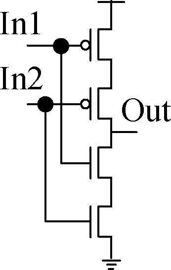
(a)
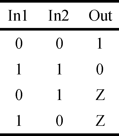
(b)
(c)
Fig.1 Circuit structure, symbol and truth table of a 2-input C-element. (a) Circuit structure; (b) Symbol; (c) Truth table
The FERST latch is based on dual-modular redundancy, since it has two identical feedback loops connecting to a 2-input C-element at the output stage. Any feedback loop employs a 2-input C-element and an inverter to retain data. Hence, the latch tolerates any SNU. However, if the output of the C-element in any feedback loop is flipped, the latch cannot self-recover, and thus the latch is neither SNU nor DNU-resilient.
The LCHR latch consists of three redundant feedback loops, one of which utilizes a keeper to directly drive its output, and two of which utilize two keepers to drive their output through a C-element at the output stage. Hence, the latch achieves SNU-tolerance but not SNU-resilience. Besides, after a simple investigation, it can be found that the latch cannot tolerate a DNU.
The DNCS latch employs six 2-input C-elements to construct a large soft error interceptive feedback loop to robustly retain data. In the feedback loop, there are many redundant nodes. Among the nodes, by feeding back three critical ones to a 3-input C-element at the output stage, the latch achieves SNU-resilience and DNU-tolerance. However, after a simple investigation, it can be found that the latch cannot self-recover from any DNU.
The NTHLTCH latch is based on triple-modular redundancy. It mainly consists of nine 2-input C-elements, sixTGs and three inverters, and hence triple interlocked feedback loops are constructed. Besides, any feedback loop comprises of three 2-input C-elements, an inverter, and a transmission gate (TG). Hence, the latch achieves SNU-and-DNU-resilience. However, after a simple investigation, it can be found that the latch is not cost-effective.
The DONUT latch is constructed by employing four interconnected dual-interlocked storage-cells (DICEs), which are self-recoverable from any SNU but not completely self-recoverable from any DNU. Due to having many interlocked redundant hold nodes, the latch achieves DNU-resilience. However, the latch is not cost-effective since no matter what mode of operation, many feedback loops are constructed, resulting in larger power dissipation.
The DeltaDICE latch consists of three interconnected DICE cells. The main difference between the DONUT latch and the DeltaDICE latch is the combination way of DICE cells.The DeltaDICE latch can provide many redundant hold nodes to robustly retain data, achieving DNU-resilience. However, similarly to the DONUT latch, the latch is not cost-effective.
2 Proposed Hardened DNURH Latch
2.1 Circuit structure and behaviour
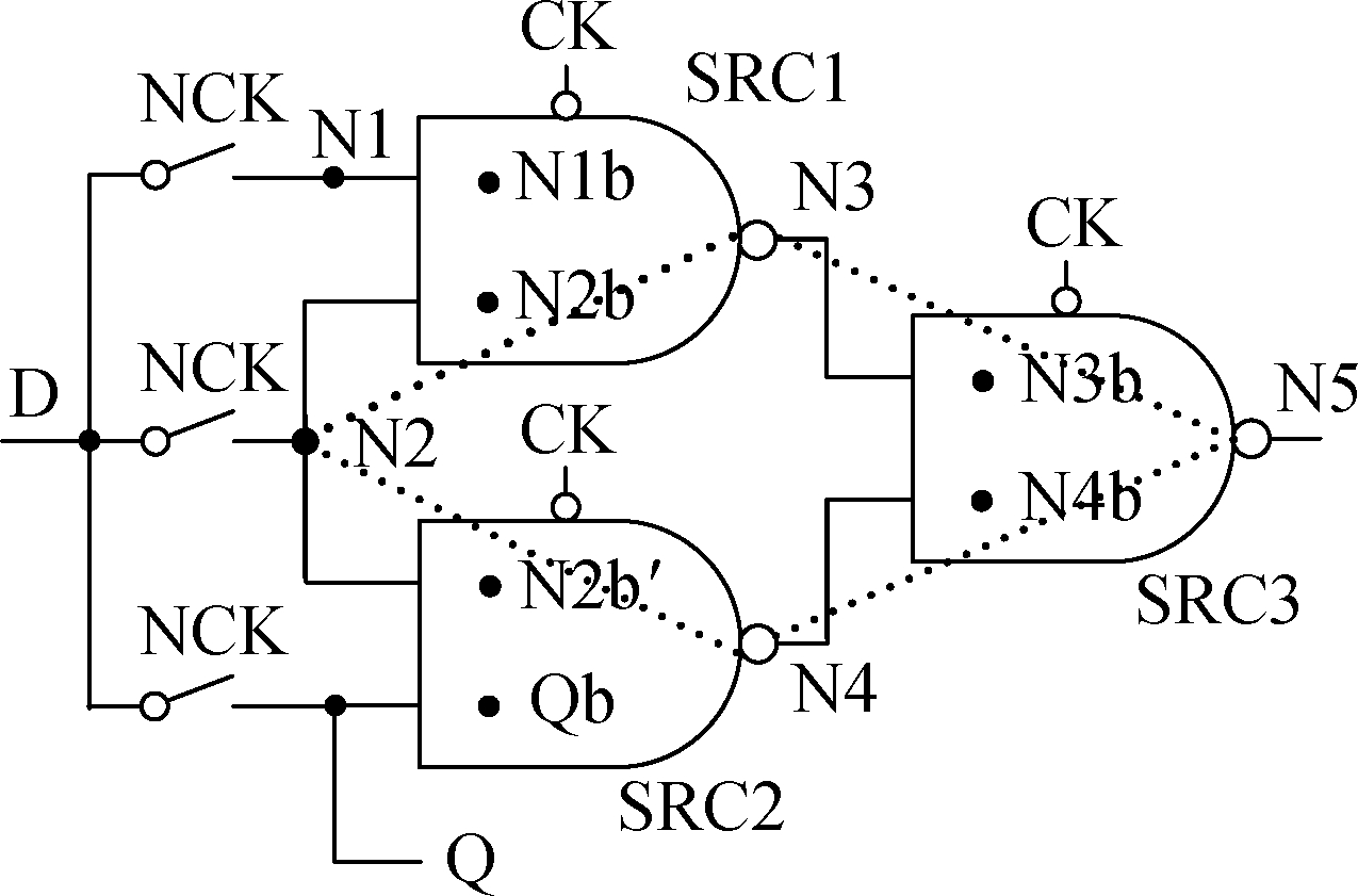
In Fig.2, the circuit structure of the proposed double-node-upset-resilient radiation-hardened (DNURH) latch is shown. It can be seen from Fig.2(c) that, the latch mainly consists of three TGs (marked as NCK since the gate-terminal of pMOS transistors are connected to NCK) and three interconnected SNU-resilient cells (SRCs) which are shown in Figs.2(a) and (b). Any SRC consists of two TGs (marked as CK since the gate-terminal of pMOS transistors are connected to CK), two inverters and three 2-input C-elements. Note that the SRC shown in Fig.2(b) comprises of three ports, in which the two ports on the left side are used for positive ones and the right side port is used for the negative one. In the latch, D, Q, CK and NCK are the input, output, system clock and negative system clock, respectively.
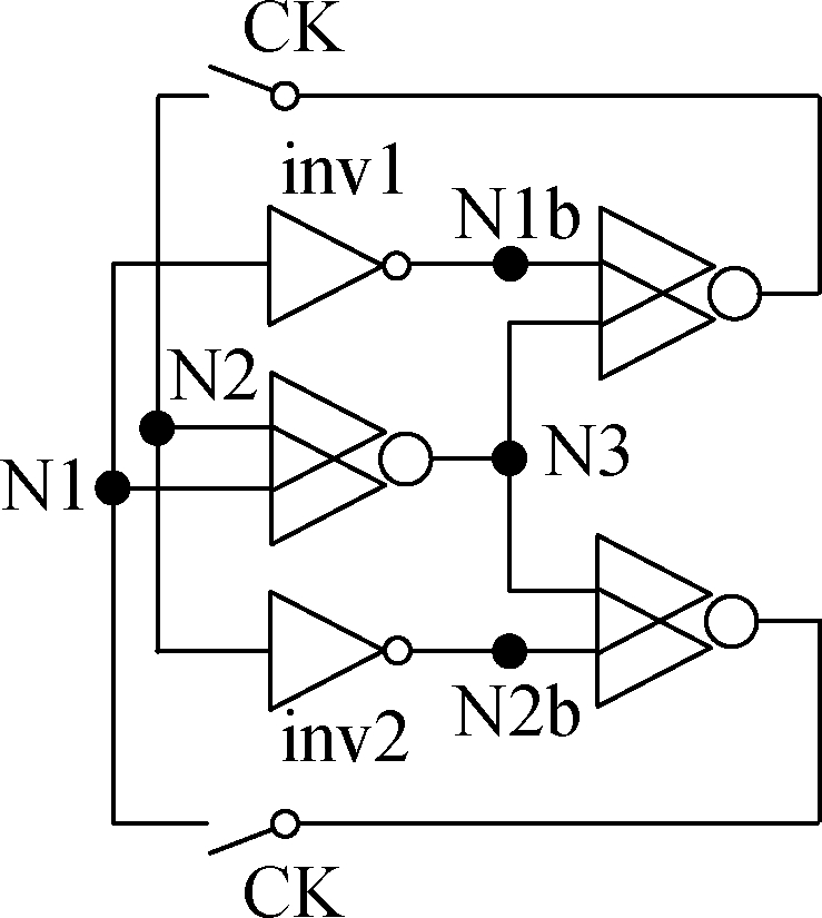
(a)
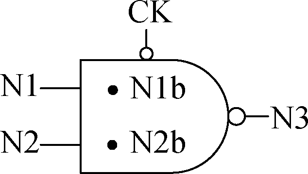
(b)
(c)
Fig.2 The proposed HLDUR latch. (a) Structure of the SRC; (b) Symbol of the SRC; (c) Structure of the HLDUR
Primarily, the error free cases are discussed. When CK=1, the latch works in a transparent mode. The positive ports of SRC1 are driven by D through TGs, and the negative port of SRC1 is driven by N1 and N2 through a 2-input C-element. As for SRC2, it is similar to SRC1. As for SRC3, the positive ports are directly driven by the negative ports of SRC1 and SRC2, and the negative port of is driven by a 2-input C-element. To avoid current competition on Q for reducing power and transmission delay, CG technology is used. Q is prevented from being driven through SRC2 but directly driven by D through a TG. Since all the positive feedback loops in the SRCs are avoided using the CG technology, the power dissipation can be saved. When CK=0, the latch works in a latching mode. N1, N2 and Q are prevented from being driven by D through TGs, and instead they are feeding back through C-elements in SRC1 and SRC2, respectively. In other words, all the feedback loops in the SRCs are constructed to retain data.
Next, the DNU-resilience is discussed. There are two cases in total: Case Ⅰ, only a single node is affected in any two SRCs (e.g. node pairs ![]() N1, N4
N1, N4![]() and
and ![]() N3b, Q
N3b, Q![]() ); Case Ⅱ, double nodes are affected in an SRC (e.g.
); Case Ⅱ, double nodes are affected in an SRC (e.g. ![]() N1, N2b
N1, N2b![]() and
and ![]() N2, N4
N2, N4![]() ). As for Case Ⅰ, since the SRCs are SNU-resilient, the affected nodes can self-recover. Therefore, the latch is DNU-resilient for Case Ⅰ.
). As for Case Ⅰ, since the SRCs are SNU-resilient, the affected nodes can self-recover. Therefore, the latch is DNU-resilient for Case Ⅰ.
As for Case Ⅱ, if the affected node pair does not match two ports of an SRC, the internal node like N1b or N2b can self-recover via the according positive port through an inverter, and thus the DNU degrades to an SNU. Since the SRCs are SNU-resilient, the latch can self-recover from the degraded SNU. Take ![]() N1, N2b
N1, N2b![]() as an example, N2b can self-recover by N2 through inv2, and then the DNU degrades to an SNU and N1 can subsequently self-recover by the correct N2b and N3 through the C-element. On the other hand, if the affected node pair matches two ports of an SRC, the SRC itself cannot self-recover the correct data. However, there are two other SRCs connecting to this SRC for ensuring enough redundant hold nodes to self-recover. Take
as an example, N2b can self-recover by N2 through inv2, and then the DNU degrades to an SNU and N1 can subsequently self-recover by the correct N2b and N3 through the C-element. On the other hand, if the affected node pair matches two ports of an SRC, the SRC itself cannot self-recover the correct data. However, there are two other SRCs connecting to this SRC for ensuring enough redundant hold nodes to self-recover. Take ![]() N2, N4
N2, N4![]() for an example, if there is no SRC1 and SRC3 connecting to SRC2, the DNU will be retained . Due to the fact that N2 is connected to SRC1, N2 can self-recover through SRC1. As for N4, the restore back process is similar to that for N2. Therefore, the latch is DNU-resilient for Case Ⅱ.
for an example, if there is no SRC1 and SRC3 connecting to SRC2, the DNU will be retained . Due to the fact that N2 is connected to SRC1, N2 can self-recover through SRC1. As for N4, the restore back process is similar to that for N2. Therefore, the latch is DNU-resilient for Case Ⅱ.
2.2 Simulation setup and verification results
The proposed DNURH latch is designed according to the 22 nm complementary-metal-oxide-semiconductor technology and the predictive technology model[14] with a supply voltage of 0.8 V and a 2 ns clock period. By means of the Cadence Virtuoso tool, the layout of the latch was drawn. Using the Synopsys HSPICE tool, simulations were performed for SNU-and-DNU-resilience verifications. In the simulations, we perform the fault injections of α particle induced SNU and DNU and hence a controllable double-exponential-current-source model is used:
(1)
where Q denotes the injected charge induced by α particle striking; τα and τβ are the time constants. In the simulations, we use the large Q up to 50 fC for a single node. τα and τβ of the current pulse are set to be 3 and 0.1 ps, respectively. Fig.3 shows the simulation results for the DNURH latch considering an error free case. It can be seen that, the operation of the latch is the same as that of a traditional static D-latch. Note that, the unrelated nodes are omitted in Fig.3.
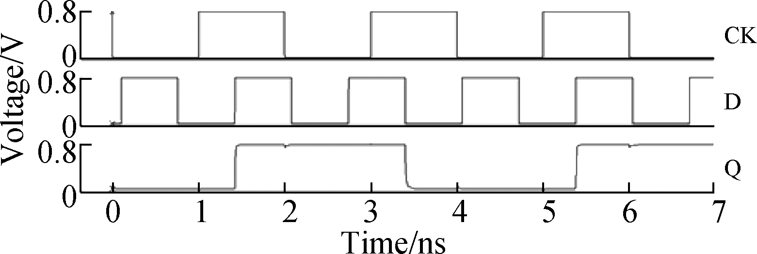
Fig.3 Simulation results for the DNURH latch considering an error free case
Fig.4 shows the simulation results for the DNURH latch considering SNUs and Case Ⅰfor DNUs. If N1 is affected, N1b will also be affected, which is the same as that for N2 to N2b, thus the simulations for N1b and N2b are omitted. Besides, the SRCs are isomorphic, thus the nodes except for the input and output ports of the SRCs can be omitted for SNU (but cannot be omitted for DNU) simulations in Case Ⅰ. The latch and the SRCs are all horizontally symmetrical, thus we can only perform the SNU simulation for nodes N3, N4, N5 and Q and the DNU simulation for ![]() N3, Q
N3, Q![]() ,
, ![]() N5, Q
N5, Q![]() ,
, ![]() N3b, Q
N3b, Q![]() and
and ![]() N4b, Q
N4b, Q![]() in Case Ⅰ. As shown in Fig.4, at 0.3, 0.7, 2.3 and 2.7 ns, an SNU is injected on N3, N5, N4 and Q, respectively, but the nodes can be restored back from the SNUs. At 4.3, 4.7, 6.3 and 6.7 ns, a DNU is injected on
in Case Ⅰ. As shown in Fig.4, at 0.3, 0.7, 2.3 and 2.7 ns, an SNU is injected on N3, N5, N4 and Q, respectively, but the nodes can be restored back from the SNUs. At 4.3, 4.7, 6.3 and 6.7 ns, a DNU is injected on ![]() N3, Q
N3, Q![]() ,
, ![]() N5, Q
N5, Q![]() ,
, ![]() N3b, Q
N3b, Q![]() and
and ![]() N4b, Q
N4b, Q![]() , respectively, but the nodes can also be restored back from the DNUs. Note that the simulated DNUs are denoted as
, respectively, but the nodes can also be restored back from the DNUs. Note that the simulated DNUs are denoted as ![]() SNUλ1, SNUλ2
SNUλ1, SNUλ2![]() , in which λ is equal to a to d, respectively.
, in which λ is equal to a to d, respectively.
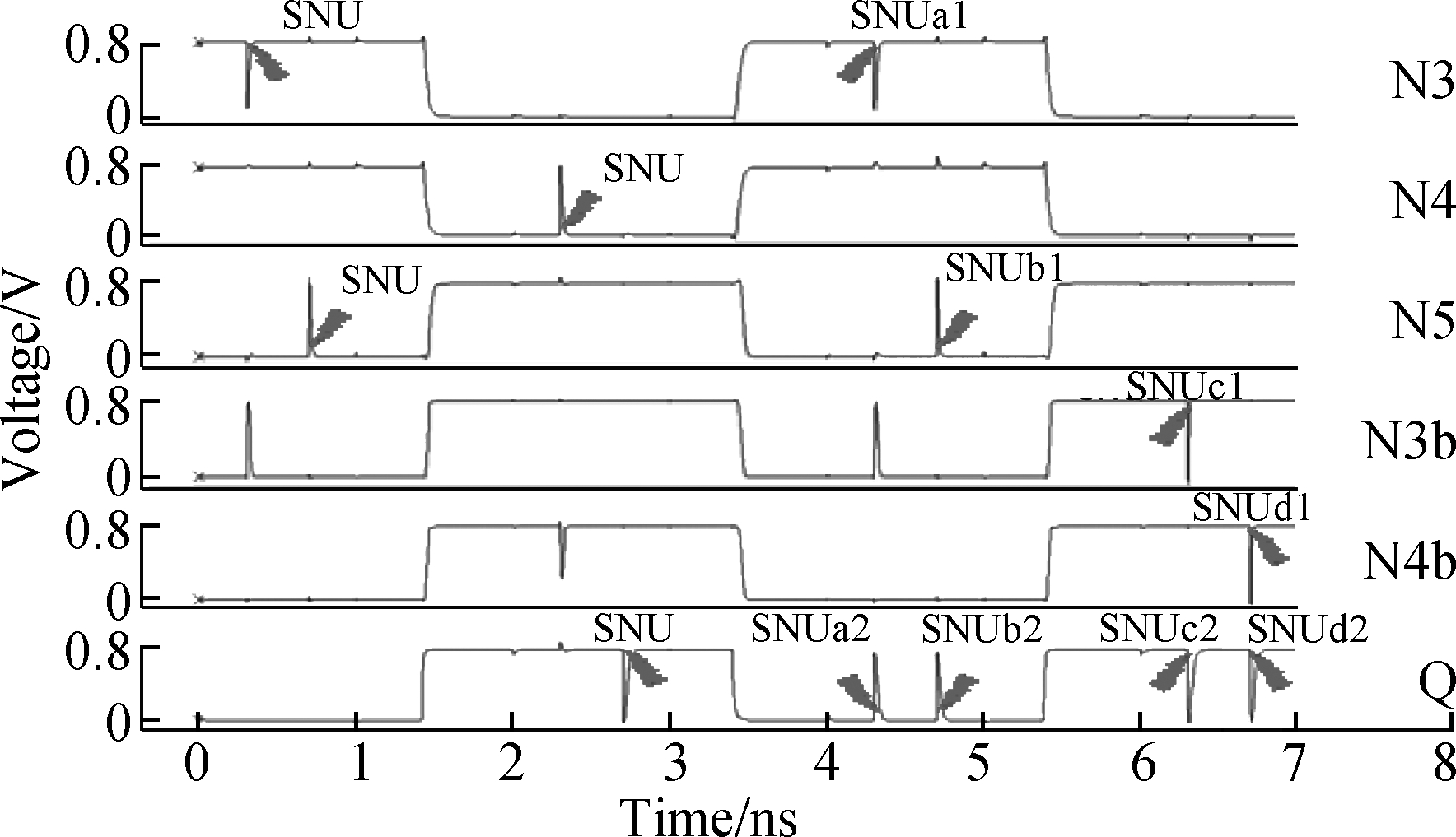
Fig.4 Simulation results for the DNURH latch considering SNUs and Case Ⅰ for DNUs
Fig.5 shows the simulation results for the DNURH latch considering Case Ⅱ and here we take SRC2 for an example. When the affected node pair does not match two of the input or output ports, ![]() N2, Qb
N2, Qb![]() ,
, ![]() N4, Qb
N4, Qb![]() ,
, ![]() Q, N2b′
Q, N2b′![]() ,
, ![]() N4, N2b′
N4, N2b′![]() and
and ![]() Qb, N2b′
Qb, N2b′![]() are simulated for DNU injections, but when the affected node pair matches two of the input or output ports,
are simulated for DNU injections, but when the affected node pair matches two of the input or output ports, ![]() N4, N2
N4, N2![]() ,
, ![]() Q, N4
Q, N4![]() and
and ![]() N2, Q
N2, Q![]() are simulated for DNU injections. As shown in Fig.5, at 0.3, 0.7, 2.3, 2.7 and 4.3 ns, a DNU is injected on
are simulated for DNU injections. As shown in Fig.5, at 0.3, 0.7, 2.3, 2.7 and 4.3 ns, a DNU is injected on ![]() N2, Qb
N2, Qb![]() ,
, ![]() N4, Qb
N4, Qb![]() ,
, ![]() Q, N2b′
Q, N2b′![]() ,
, ![]() N4, N2b′
N4, N2b′![]() and
and ![]() Qb, N2b′
Qb, N2b′![]() , respectively, but the node pairs can self-recover. At 4.7, 6.3 and 6.7 ns, a DNU is injected on
, respectively, but the node pairs can self-recover. At 4.7, 6.3 and 6.7 ns, a DNU is injected on ![]() N4, N2
N4, N2![]() ,
, ![]() Q, N4
Q, N4![]() and
and ![]() N2, Q
N2, Q![]() , respectively, but the node pairs can also self-recover. Note that the injected DNUs are denoted as
, respectively, but the node pairs can also self-recover. Note that the injected DNUs are denoted as ![]() SNUλ1, SNUλ2
SNUλ1, SNUλ2![]() , in which λ is equal to a to h, respectively. From the above simulations, it can be seen that the DNURH latch is both SNU and DNU resilient.
, in which λ is equal to a to h, respectively. From the above simulations, it can be seen that the DNURH latch is both SNU and DNU resilient.
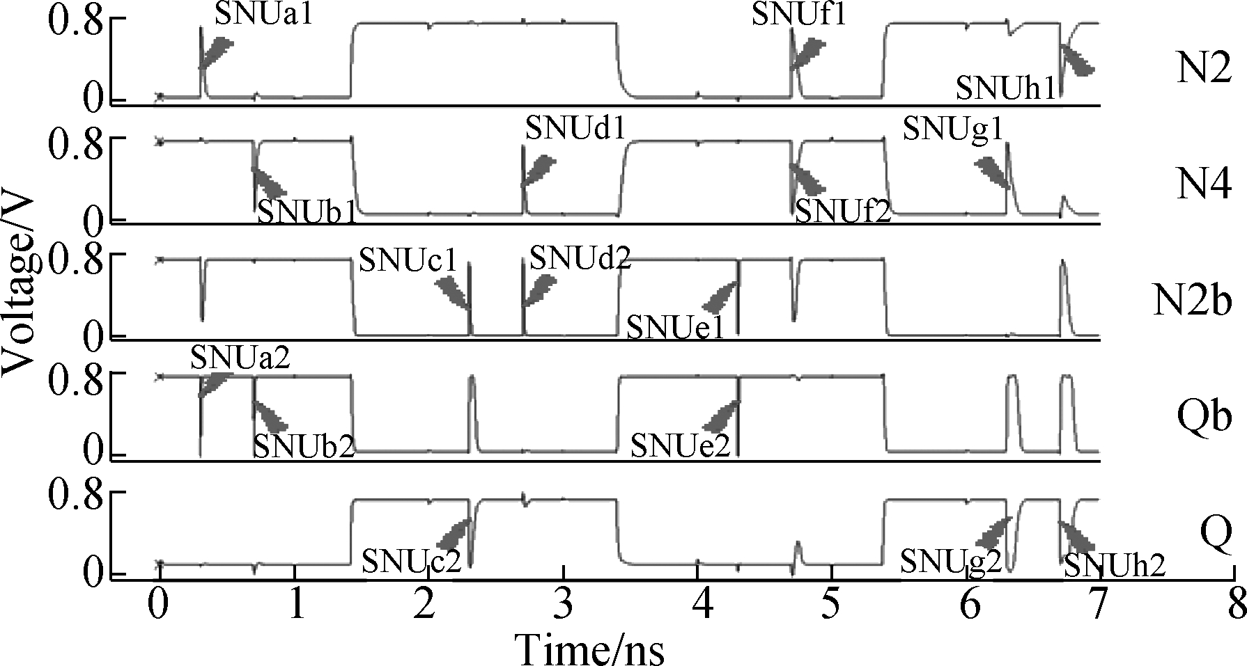
Fig.5 Simulation results for the DNURH latch considering Case Ⅱ for DNUs
3 Latch Comparison and Evaluation
To quantitatively evaluate overheads of the proposed DNURH latch and make a comparison with the existing latches, we similarly performed the simulations for the latches mentioned in Section 1 (FERST[5], LCHR[8], DNCS[9], NTHLTCH[10], DONUT[11] and DeltaDICE[12]) using the same technology. The transistor sizes of the latches are optimized to reduce overheads, especially, on the silicon area. Here, we take the optimized transistor sizes of the C-elements for an example. The W/L of the PMOS transistor is 90/22 nm while the W/L of the NMOS transistor is 28/22 nm. Tab.1 shows the comparison results of the hardened latches.
Tab.1 Comparison results of hardened latches
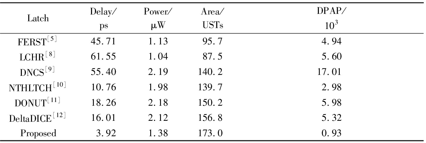
LatchDelay/psPower/μWArea/USTsDPAP/103FERST[5]45.711.1395.74.94LCHR[8]61.551.0487.55.60DNCS[9]55.402.19140.217.01NTHLTCH[10]10.761.98139.72.98DONUT[11]18.262.18150.25.98DeltaDICE[12]16.012.12156.85.32Proposed3.921.38173.00.93
In Tab.1, the data in the first column denote the latch names; the data in the second to the fifth columns denote the D-to-Q transmission delay, the average of static plus dynamic power dissipation, silicon area, and delay-power-area product (DPAP)[13], respectively. Similarly, the silicon area is measured with equivalent unit size transistors (USTs)[9, 13], and the DPAP metric was calculated by multiplying the delay, power, and silicon area. It can be found that, a smaller DPAP is better.
It can be seen from Tab.1, to achieve SNU and DNU resilience of the proposed latch, more silicon area has to be used compared with the other hardened latches. The proposed latch has the smallest transmission delay and DPAP due to the use of a direct transmission path from D to Q as well as the CG technology. Compared with the NTHLTCH, DONUT and DeltaDICE latches which are SNU-and-DNU-resilient, the proposed latch has the smallest transmission delay, power dissipation, and the DPAP, which validates the cost effectiveness of the proposed latch except for the silicon area overhead.
In a quantitative point of view, it can be found from Tab.1 that compared with the up-to-date DNU-resilient latches, the proposed latch reduces transmission delay by 72.54%, power dissipation by 33.97% and DPAP by 78.57% with the cost of only 16.45% silicon area increase on average. Note that, the percentage data for delay is calculated as
(2)
Hence, the percentage data for power dissipation, silicon area, and DPAP were calculated. It can be found that although the same type latches can be highly reliably operated, they have larger cost penalties, especially, for transmission delay, power dissipation and DPAP. In summary, the proposed latch can be highly robustly operated and has lower overheads.
4 Conclusion
As technology scaling, particle-striking induced SNU and DNU in latches are becoming serious. This paper proposed a novel DNU-resilient radiation-hardened latch in 22 nm complementary-metal-oxide-semiconductor technology. The latch mainly comprises of three single-node-upset-resilient cells to construct many redundant nodes to achieve DNU-resilience. Simulation results demonstrate the DNU-resilience of the latch and also show that the latch has lower costs for transmission delay, power dissipation and DPAP on average compared with the up-to-date DNU-resilient latches.
[1]Ferlet-Cavrois V, Massengill L W, Gouker P. Single event transients in digital CMOS—A review [J].IEEE Transactions on Nuclear Science, 2013, 60(3): 1767-1790. DOI:10.1109/tns.2013.2255624.
[2]Huang Z F, Liang H G, Hellebrand S. A high performance SEU tolerant latch [J]. Journal of Electronic Testing, 2015, 31(4): 349-359. DOI:10.1007/s10836-015-5533-5.
[3]Lin S, Kim Y B, Lombardi F. Design and performance evaluation of radiation hardened latches for nanoscale CMOS [J]. IEEE Transactions on Very Large Scale Integration Systems, 2011, 19(7): 1315-1319. DOI:10.1109/tvlsi.2010.2047954.
[4]Nan H Q, Choi K. High performance, low cost, and robust soft error tolerant latch designs for nanoscale CMOS technology [J]. IEEE Transactions on Circuits and Systems I: Regular Papers, 2012, 59(7): 1445-1457. DOI:10.1109/tcsi.2011.2177135.
[5]Fazeli M, Patooghy A, Miremadi S, et al. Feedback redundancy: A power efficient SEU-tolerant latch design for deep sub-micron technologies [C]//37th Annual IEEE/IFIP International Conference on Dependable Systems and Networks. Edinburgh, UK, 2007: 276-285. DOI:10.1109/dsn.2007.51.
[6]Namba K, Sakata M, Ito H. Single event induced double node upset tolerant latch [C]//IEEE 25th International Symposium on Defect and Fault Tolerance in VLSI Systems. Kyoto, Japan, 2010: 280-288. DOI: 10.1109/DFT.2010.41.
[7]Watkins A, Tragoudas S. Radiation hardened latch designs for double and triple node upsets [J]. IEEE Transactions on Emerging Topics in Computing, 2018, to appear. doi:10.1109/TETC.2017.2776285.
[8]Qi C H, Xiao L Y, Guo J, et al. Low cost and highly reliable radiation hardened latch design in 65 nm CMOS technology [J]. Microelectronics Reliability, 2015, 55(6): 863-872. DOI:10.1016/j.microrel.2015.03.014.
[9]Katsarou K, Tsiatouhas Y. Soft error interception latch: double node charge sharing SEU tolerant design [J]. Electronics Letters, 2015, 51(4): 330-332. DOI:10.1049/el.2014.4374.
[10]Li Y, Wang H B, Yao S, et al. Double node upsets hardened latch circuits [J]. Journal of Electronic Testing, 2015, 31(5/6): 537-548. DOI:10.1007/s10836-015-5551-3.
[11]Eftaxiopoulos N, Axelos N, Pekmestzi K. DONUT: A double node upset tolerant latch [C]// IEEE Computer Society Annual Symposium on VLSI. Montpellier, France, 2015: 509-514.
[12]Eftaxiopoulos N, Axelos N, Zervakis G, et al. Delta DICE: A double node upset resilient latch [C]//IEEE International Midwest Symposium on Circuits and Systems. Colorado, USA, 2015: 1-4.
[13]Yan A B, Huang Z F, Yi M X, et al. Double-node-upset-resilient latch design for nanoscale CMOS technology[J]. IEEE Transactions on Very Large Scale Integration Systems, 2017, 25(6): 1978-1982. DOI:10.1109/tvlsi.2017.2655079.
[14]The Nanoscale Integration and Modeling (NIMO) Group at ASU. Predictive technology model (PTM) [EB/OL]. (2011-06-01)[2017-06-12].http://ptm.asu.edu/.