With the development of technology, the demand of improved performance in the semiconductor transistor has required reducing the device’s dimension in recent years, which follows a well-known scaling law known as “Moore’s law”. The size of the device is further reduced to its physical limit, and the research of small size effect is essential[1-2]. The dominance of Si in microelectronics is largely based on the high quality of the interface between Si and its native oxide SiO2[3].Many studies have been devoted to replacing SiO2 with high-k gate dielectrics. However, in the case of high-k gate dielectrics, very thin SiO2 is unavoidable[4-5]. Si- and SiO2-based systems also have the advantage of low cost as well as dealing with abundant, nontoxic, stable and durable materials. Therefore, many experiments and theoretical verifications on Si/SiO2 interface have been carried out[6-12]. However, the precise bonding information remains controversial[12-15].
So far, there has been much research about the Si/SiO2 interface structure and electrical properties, and many models have been built[16-18], but these studies mainly focus on using the first principle or other means[19-21] to explore the physical and chemical properties of the interface itself, the impact of the defects or doping on the interface. For example, Wen et al.[22] have used ReaxFF molecular dynamics (MD) simulations to investigate the atomic mechanism of tribo-chemical wear of silicon at the Si/SiO2 interface; Ono et al.[23] calculated the electronic structure and dielectric properties of interface; Kova![]() evi
evi![]() et al.[11] researched the structure, defects and the stress on the Si/SiO2, and so on[24-26]. However, the research on the properties of transistor is scarce, and the finite size effect is seldom considered in transistor analysis[27-31]. In this paper, we study the influence of the Si/SiO2 interface on the characteristics of ultra-thin gate transistor considering the finite size effect. The results will provide a theoretical basis for the application of nano-scale silicon based transistor.
et al.[11] researched the structure, defects and the stress on the Si/SiO2, and so on[24-26]. However, the research on the properties of transistor is scarce, and the finite size effect is seldom considered in transistor analysis[27-31]. In this paper, we study the influence of the Si/SiO2 interface on the characteristics of ultra-thin gate transistor considering the finite size effect. The results will provide a theoretical basis for the application of nano-scale silicon based transistor.
1 First Principle Method
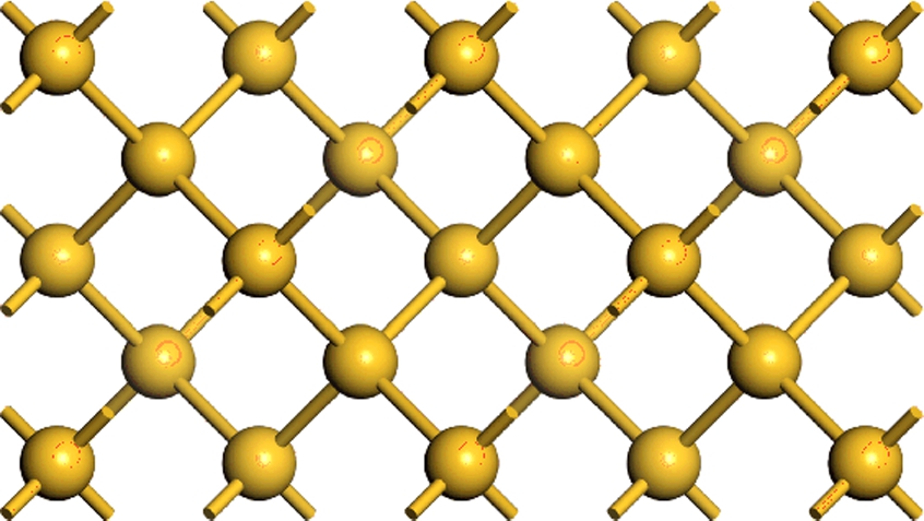
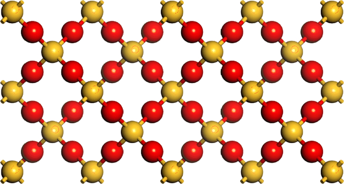
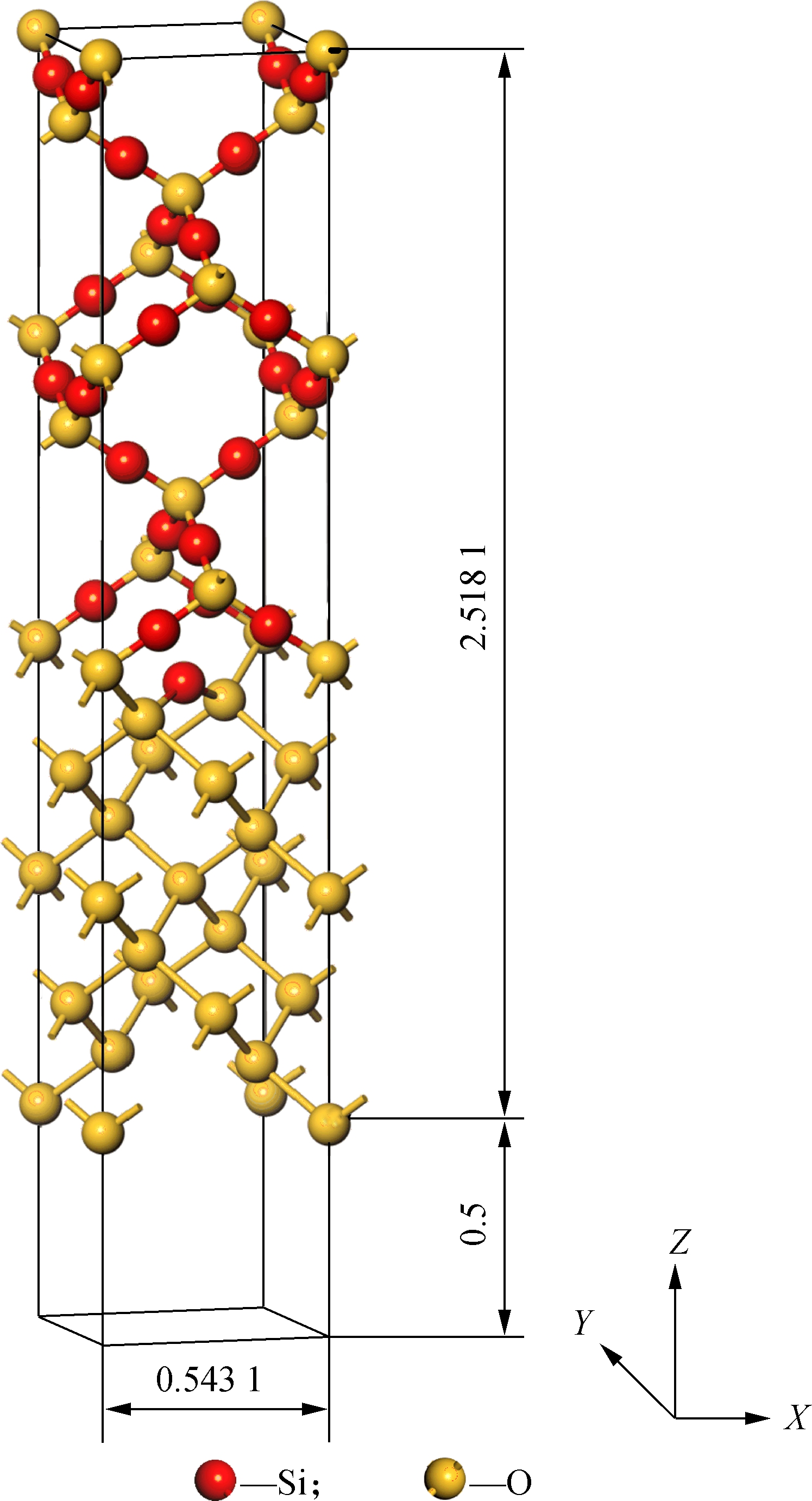
The interface model used in this paper is the bridge-oxygen model (BOM), which is first put forward by Herman et al[32]. It is the simplest and most suitable model for electronic structure calculation[33-36]. This model consists of two layers of Si(see Fig.1 (a)) and two layers of idealized β-cristobalite SiO2(see Fig.1 (b)). The experiment lattice constants are 0.543 and 0.716 nm for Si and SiO2, respectively. The lattice mismatch rate is 32%. The mismatch can be reduced to less than 7% by rotating SiO2 by an angle of π/4, as shown in Fig.1(c). The BOM interface dangling bonds are saturated by adding an oxygen atom to bridge the two Si bonds. Here, the Si-O-Si angle is 144° and the length of Si-O bonds is 0.202 nm. The resulting unit cell has 72 atoms (47 Si and 25 O atoms)and dimensions of 0.5431 nm in the X-Y plane and 2.5181 nm in the Z (growth) direction. To ensure the independence of the interface, a 0.5 nm vacuum layer is added. Finally, the interface structure is obtained in Fig.1(d). No cell optimization of the model has been carried out.
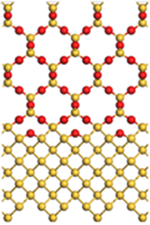
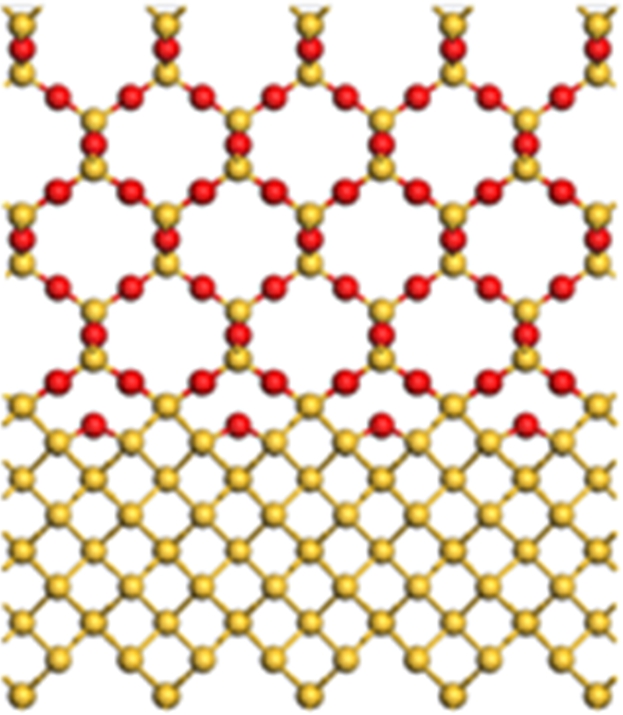
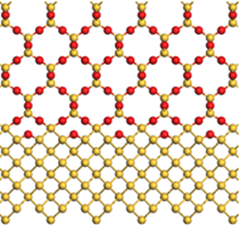
In order to study the characteristics of the interface in nano-scale transistor considering the finite size effect, six structures with different sizes are constructed, as shown in Fig.2.
The geometrical optimization and energy calculations are performed using the CASTEP (Cambridge serial total energy package) program[37], which employs the plane pseudopotential method to calculate the total energy within the framework of the Kohn-Sham DFT. The PBE (Perdew, Burke, Ernzerh) formulation of the generalized gradient approximation (GGA) is always used to describe exchange correlation energy[38]. The Vanderbilt ultra-soft pseudo potential is used, which allows numerically converged calculations at relatively low kinetic energy cutoffs of the plane wave basis. The Broyden, Fletcher, Goldfarb and Shanno (BFGS) algorithm is applied to optimize the model structures. The convergence criteria for the self-consistent field (SCF) energy and the displacement are set to be 2.0×10⁻⁶ eV/atom and 2×10⁻⁴ nm. 2×5×1 k-point meshes are taken in the Brillouin zone, and the ground state energy is calculated with the Pulay density mixed method under the following conditions: The precision is 1.0×10⁻⁵ eV/atom, and the cutoff energy of the plane wave is 340 eV.
Using the DFT theory, the effect of dimensional changes on the characteristics has been studied. Jie et al.[39] used CASTEP to study the influence of GaSe layer variation on optical properties. Niedfeldt et al.[40] also reported the influence of different cell sizes.
2 Results and Discussion
2.1 Electronic structure
It has been pointed out that the change of Si layer will affect the properties of silicon-based devices[41]. Therefore, the influence of the varied w/t on the Si-Si and Si-O bond length in the interface is first calculated.
Fig.3 shows the average bond length of Si-Si and Si-O. As seen from Fig.3, the average bond length of Si-Si gradually decreases with the increase in w/t, and finally tends to be saturated. On the other hand, although the Si-O bond length increases with the increase in w/t, it also finally tends to be saturated. These results show that the interface structure tends to be stable due to the influence of the surface state and quantum size effect with the increase in w/t[42].The relative change of the Si-Si bond length achieved 3.16%, and the Si-O bond length is as high as 4.53%. Such a large change is very important to the nano-scale transistor. From Fig.3, we conclude that the finite size effect can be ignored when the width is up to 2 nm and above when the oxide thickness is 2.5 nm.
2.2 Optical properties
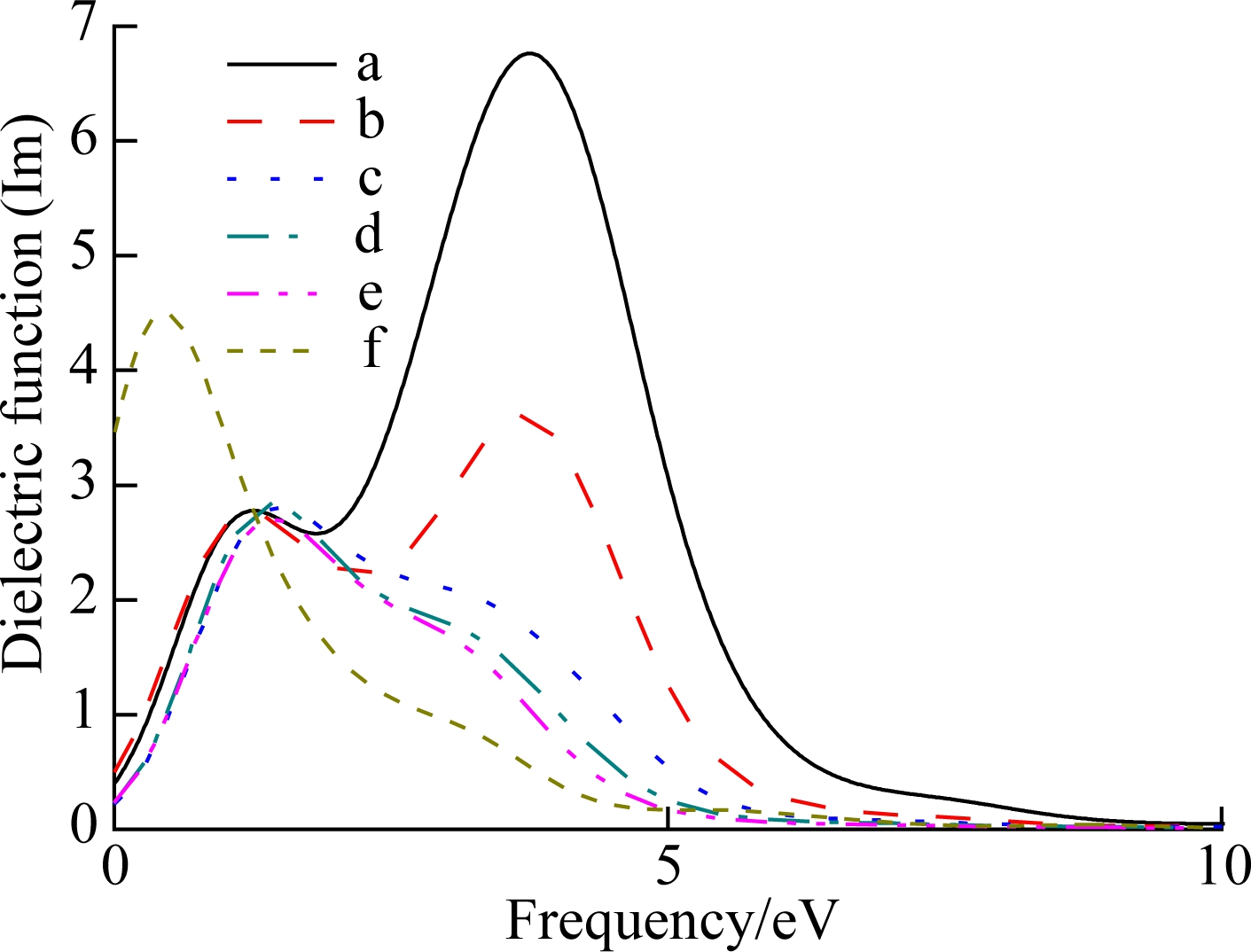
By analyzing the electronic structure of the interface, it is found that the increase in w/t will affect the bond length of the Si side. The change of the structure in the Si side will inevitably affect the optical properties of the interface[41]. The dielectric function is the bridge between the microphysical processes of interband transitions and the electronic structure of materials.ω is the independent variable of the complex dielectric function, ε(ω)=ε1(ω)+iε2(ω), ε1(ω) is the real part and ε2(ω) is the imaginary part of the dielectric function. It mainly represents the transition between the occupied and non-occupied states of electrons, and other spectral information can be easily obtained from it. Therefore, the imaginary part of the dielectric function and the other optical parameters are calculated and analyzed.
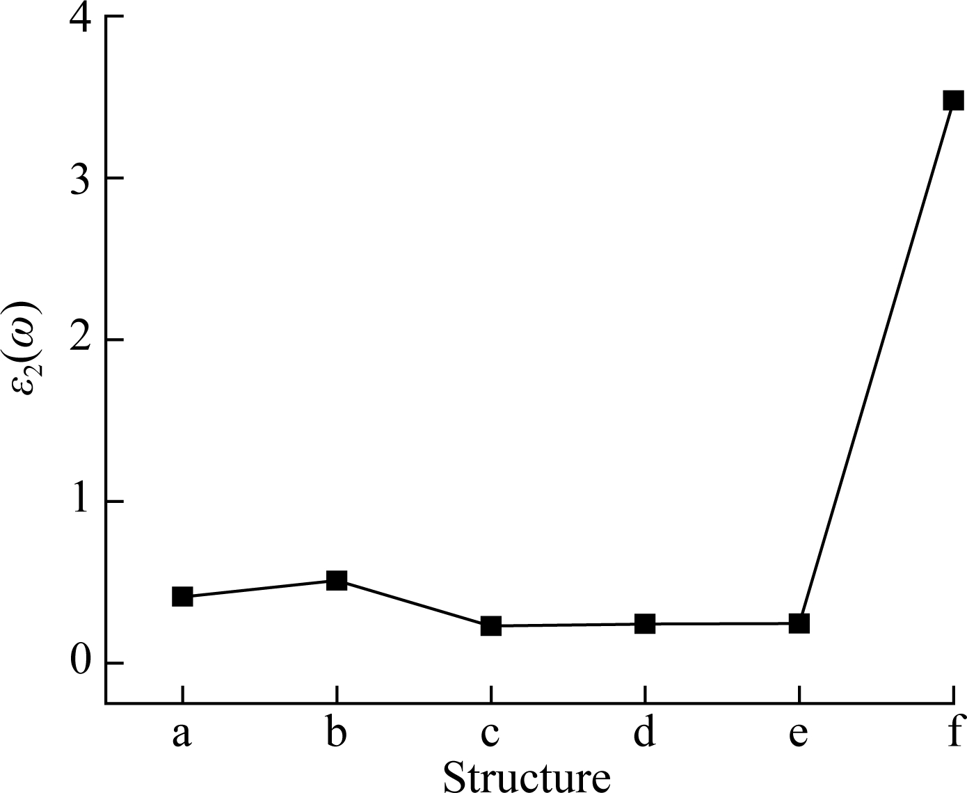
The changes in the imaginary part of dielectric function under different ratios of w/t are given in Fig.4. It can be seen that the absorption peak shifts to the left and the peak value decreases gradually with the increase in w/t.
Fig.5 shows the variation of absorption peak with the increase in w/t. It can be seen that the absorption peak shifts to the left and decreases gradually with the increase in w/t. It indicates that with the increase in w/t, the absorption of photon energy in the high-energy region becomes weaker due to the influence of the surface effect and the quantum size effect. By comparing structure a with structure f, the absorption peak has decreased by almost an order of 10-1. This property can be used to control the optical properties of the transistor.
The change of optical properties with ratio w/t will lead to the change of electronic properties of devices. Therefore, we next investigate the tunneling current of the nano-scale transistor consisting of the Si/SiO2 interface with different w/t.
(a)
(b)

(c)
(d)
Fig.1 The BOM model. (a) Two layers of Si; (b) Two layers of idealized β-cristobalite SiO2; (c) Rotating SiO2 by an angle of π/4; (d) The model structure considered in the present study(unit: nm)
![]()
(a)

(b)
(c)
(d)
(e)

(f)
Fig.2 The structures of six nano-sizes with different ratios of channel width to thickness (w/t). (a) w/t=1×5.431/25.181; (b) w/t=2×5.431/25.181; (c) w/t=3×5.431/25.181; (d) w/t=4×5.431/25.181; (e) w/t=5×5.431/25.181; (f) w/t=6×5.431/25.181
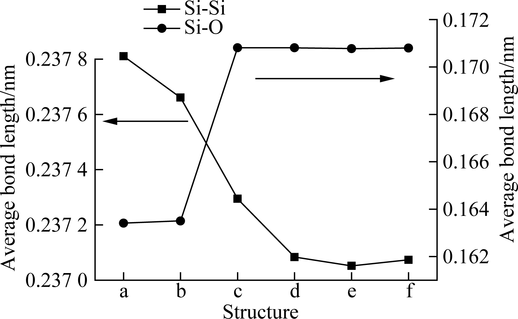
Fig.3 The average bond length of Si-Si and Si-O for the six nano-sizes
(a)
(b)
Fig.4 The dielectric function. (a) The dielectric function in Si/SiO2 interface for the six nano-sizes; (b) The imaginary part of the dielectric function

Fig.5 The size dependence of the absorption in Si/SiO2 interface
2.3 Energy band profile
2.3.1 Planar microscopic potential via first principles
The valence band profiles are calculated using the average potential method[43]. The electrostatic potential for the super cell is averaged in the X-Y plane; then, a planar microscopic potential is calculated in the Z direction.
(1)
At the Si/SiO2 interface, the band changes continuously from Si to SiO2 (see Fig.6). The coordinates Z1, Z2 are corresponding to the transition region boundaries and D is the width of the transition region. Before the calculation of transistor characteristics, the definition of the transition region is very important. The coordinates in the Z direction, corresponding to the band profile changes in a trend away from the averages and vice versa, are set to be the interface region boundaries. For example, the band goes up away from its average at point A in Fig.6, so the coordinate Z1 corresponding to point A can be set to be a boundary for the interface structure. Similarly, the other boundary can be set at Z2. After measurement, we can obtain the width of the transition region, which is D=Z2-Z1=0.48 nm. This result is consistent with others reported[16,26,36,44-45] and it is also in agreement with the measured results in the laboratory[46]. By measuring the potential of the structure with six nano-sizes (see Fig.2) in this paper, D remains unchanged at different ratios of w/t.
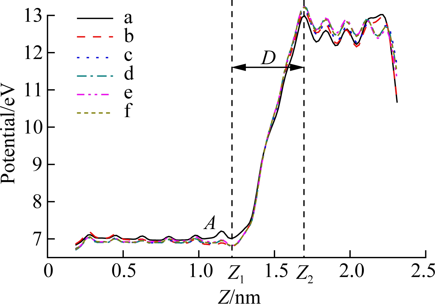
Fig.6 The planar microscopic potential along the Z direction
We can measure the VBM for the six structures with different sizes in Fig.6, and further obtain the CBM of these structures. The barrier heights are shown in Fig.7 which are calculated according to Fig.6. It can be seen clearly that the barrier height curve shows a downward trend, and the trend is getting slower. It is clear that the tunneling current will increase with the increase in w/t due to the reduction of the barrier height.
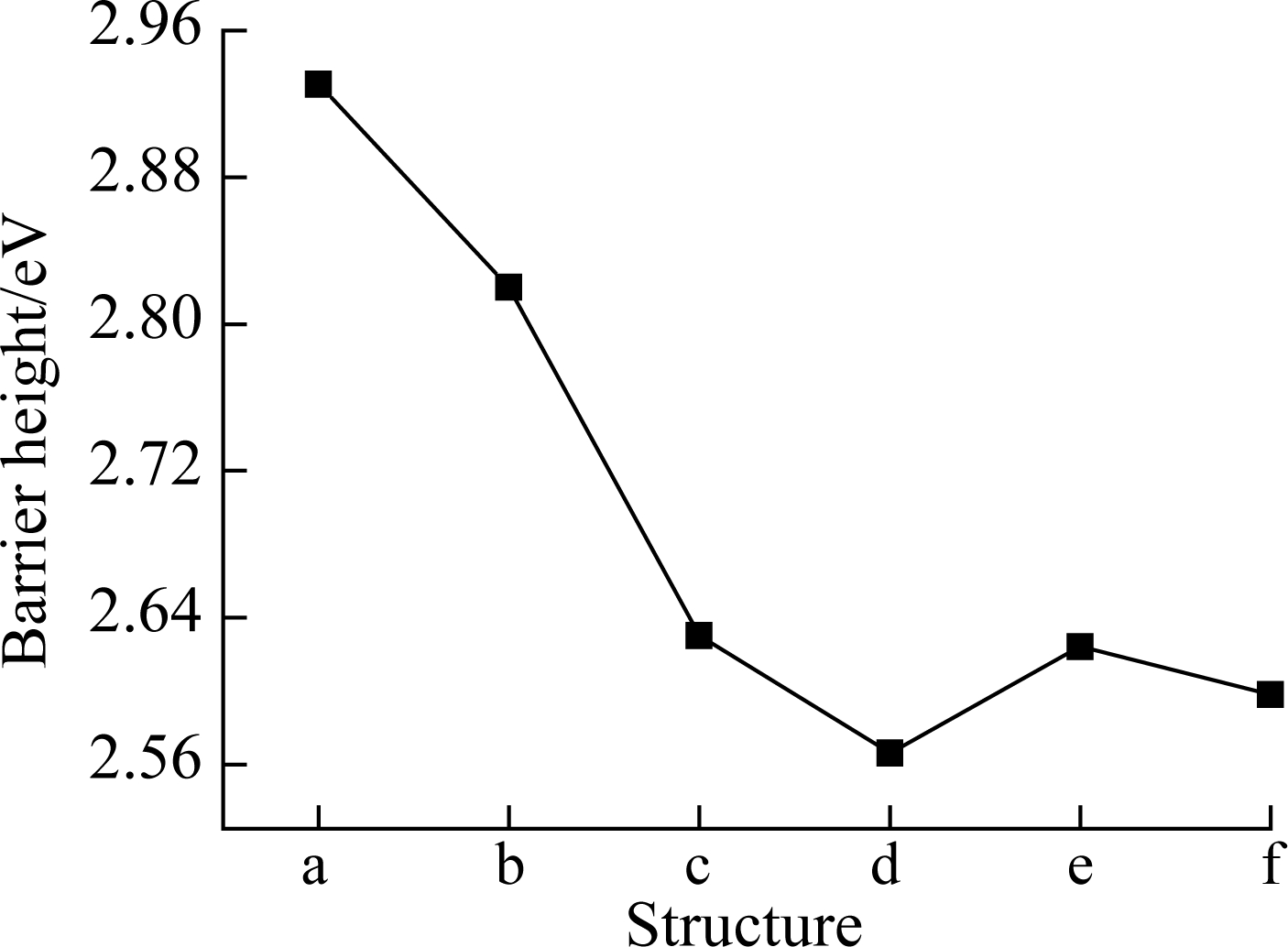
Fig.7 The barrier height for the six nano-sizes
2.3.2 Gate tunneling current
Ando and Itoh[47] presented a numerical calculation method for gate leakage current with two tunneling conditions:
(2)

(3)
where Vox is the voltage added to the barrier layer, and the electric field in the oxide is Eox=Vox/Tox. Toxis the oxide thickness. B and C are given, respectively, by
(4)
(5)
where q is the free electron charge; φ is the potential barrier height (eV)at the metal-oxide interface ignoring the effect of the image potential; ![]() is reduced Plank’s constant; m is the free electron mass;
is reduced Plank’s constant; m is the free electron mass; ![]() is the effective mass of electrons in the conduction band in oxide.
is the effective mass of electrons in the conduction band in oxide.
The above classical tunneling current formulae approximately consider the interface region to be abrupt, and do not consider the influence of image potential. However, it can be clearly seen that the potential changes in the interface are not abrupt as shown in Fig.6. On the other hand, it will reduce the area and the thickness of the barrier due to the existence of the image potential. This will cause an increase in the tunneling current. Furthermore, when the oxide layer becomes ultra-thin and the applied voltage is below the potential barrier height, the classical FN formula is not applicable[48].
Taking the transition region (width D) into account, the FN tunneling current through a triangular barrier can be rewritten as[49]
(6)
where
(7)
Taking the effect of barrier lowering induced by image potential into account, the direct tunneling (DT) current can be rewritten as[48]
(8)
where φeff=φ-Eox.The transition region width D is calculated according to Fig.6. The barrier heights without electric field(φ) are also given for the six structures in Fig.7. Other parameters used in this work are ![]() m,
m,![]() =h/(2π),D=0.48 nm.
=h/(2π),D=0.48 nm.
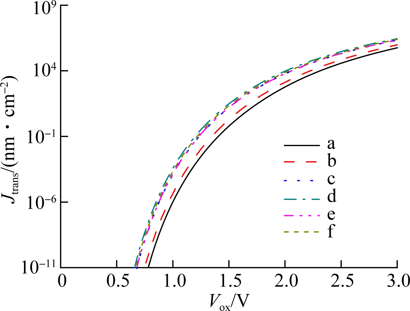
Using Eq.(6), the FN tunneling current considering the transition region can be obtained in Fig.8(a). It shows the FN tunneling current under different applied voltages across gate oxide with different ratios of w/t. It can be seen that the tunneling current increases gradually with the increase in the ratio, but the trend of the increase decreases, which is corresponding to the observed electronic structure (see Fig.3). In Fig.8(b), the change in the ratio of Jtrans/Jtrans0 as a function of the applied gate voltages is calculated, where Jtrans0 is the FN tunneling current without the finite size effect. The FN tunneling current becomes larger considering the finite size effect than that without considering. The ratio decreases with the increase in the electric field of the oxide layer. When the electric field is 10 MV/cm, the ratio of Jtrans/Jtrans0 is up to 45 for structures with different sizes. However, when the field increases to 20 MV/cm, the ratio is only 4. Clearly, the FN tunneling current will increase due to the finite size effect. The increased amount becomes smaller when the electric field is increased.
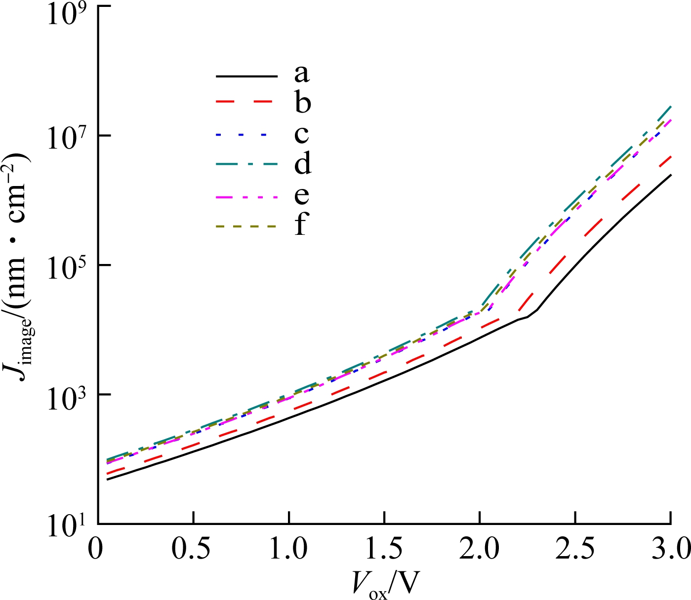
Fig.9(a) shows the change of Jimage, which is calculated using Eq.(8). It can be seen that the direct tunneling current already exists in the low voltage region which is different from the FN tunneling current. The direct tunneling current will increase with the increase in w/t. We can also see that the currents have an obvious turning point in the high voltage region, and the current increases significantly after the turning point. In an ultra-thin gate transistor, the gate field will increase with the decrease of the gate thickness, which corresponds to the high voltage region in which the direct tunneling current is significantly increased. Through this result, we find that the effect caused by sizes cannot be ignored as the size of the transistor decreases.
(a)

(b)
Fig.8 The FN tunneling current as a function of the applied voltage across gate oxide with different w/t for the six structures(Tox=1.62 nm). (a) The change of Jtrans; (b) The change in the ratio of Jtrans/Jtrans0
Fig.9(b) shows the change in the ratio of Jimage/Jimage0, where Jimage0 is the direct current without the finite size effect. It can be seen that the direct current will increase due to the finite size effect. It also shows that with the increase in gate voltage, there are two turning points in the current curve. When near the FN tunneling area, the influence of the finite size effect is almost saturated and declines. This indicates that the influences of the finite size effect on the direct tunneling and FN tunneling are different. When the electric field is 10 MV/cm, the ratio of Jimage/Jimage0 is only 3 for structures with different sizes. We can conclude that the finite size effect has a greater impact on the FN tunneling current than on the direct tunneling current.
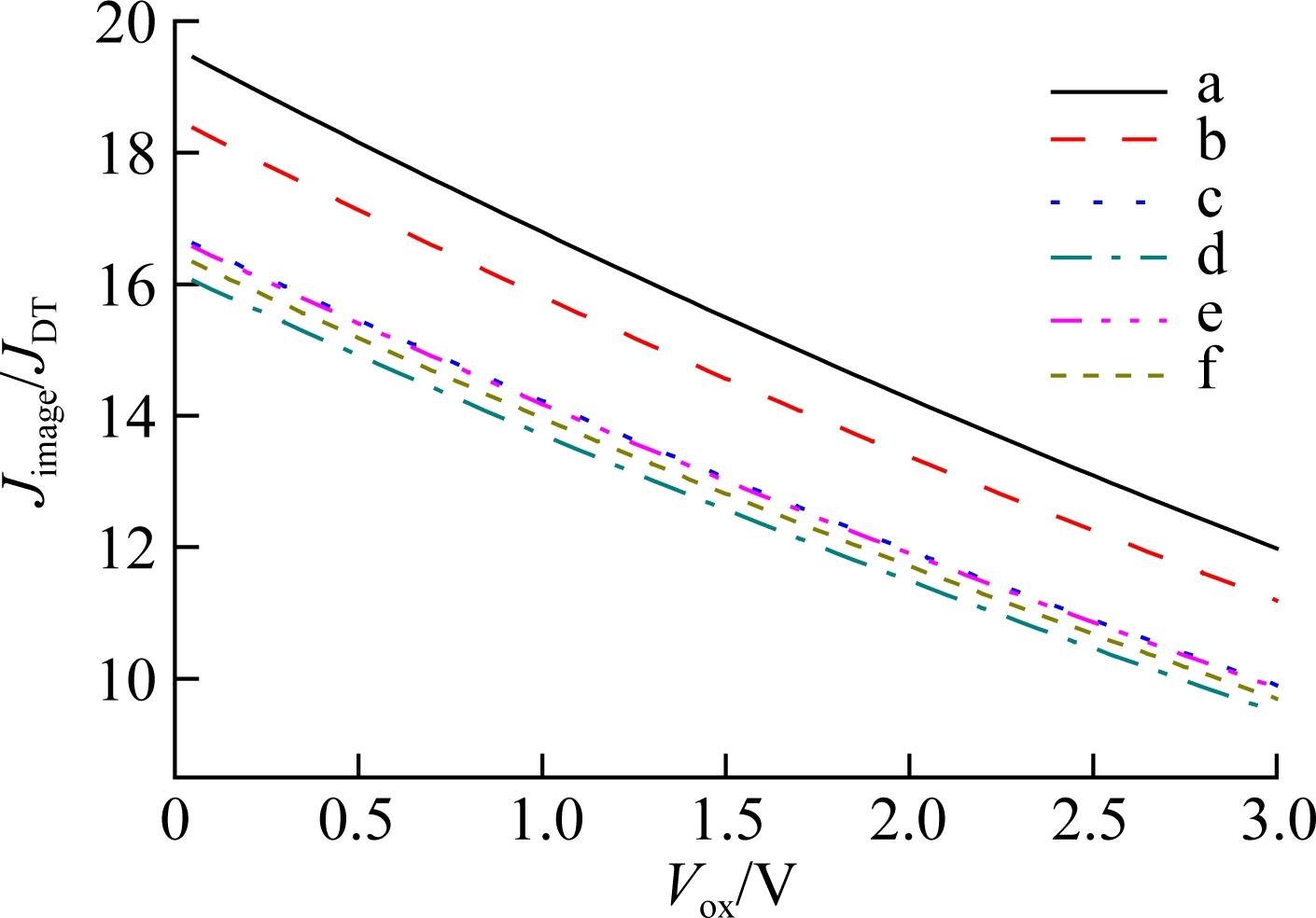
Figs.10(a) and (b) show the changes in the ratios of Jtrans/JFN and Jimage/JDT, where JFN is the tunneling current without the transition region, and JDT is the direct tunneling current without considering the effect of image potential. It can be seen that both the tunneling current will increase with the transition region and image potential. However, the existence of the finite size effect has redu-ced the influence of the transition region and image potential, and leads to a decrease in the ratio of Jtrans/JFN and Jimage/JDT, separately. It also shows that with the increase in gate voltage, both Jtrans/JFN and Jimage/JDTwill gradually decrease.
(a)

(b)
Fig.9 The direct tunneling current as a function of the applied voltage across gate oxide. (a) The change of Jimage; (b) The change in the ratio of Jimage/Jimage0
Fig.11(a) shows the change in the ratio of Jtrans/JFN, in which the currents are calculated under different gate voltages and oxide thicknesses when the barrier height is φ=3.15 eV. It can be seen that the influence of the transition region on the tunneling current decreases with the increase in the gate voltage under the same oxide thickness. Furthermore, the degree of decline will gradually increase with the decrease of the oxide thickness. The ratio of Jtrans/JFN decreases from 7.8 to 4.5 with Tox=1 nm when the gate voltage changes from 0 to 3 V. On the other hand, the ratio decreases from 7.8 to 6.8 with Tox=3.5 nm when the gate voltage changes from 0 to 3 V. This is because with the decrease in thickness, the transition region occupies a larger proportion of the whole interface region. Therefore, considering the transition region or not will produce a greater impact on the tunneling current when the oxide thickness is smaller.
Fig.11(b) shows the change in the ratio of Jimage/JDT under different gate voltages and oxide thicknesses, separately. Comparing Fig.11(a) and (b), we find that alth-ough the ratio is greater for direct tunneling current than for the FN tunneling current at the same oxide thickness and same gate voltage, the variation trend is similar, which is consistent with the numerical results obtained by Mao et al[48]. Jimage/JDT decreases with the increase in gate voltage. We also conclude that considering the image potential or not will produce a greater impact on the tunneling current when the oxide thickness is smaller. The ratio of Jimage/JDT decreases from 21.6 to 9.7 when the gate voltage changes from 0 to 3 V. This ratio is lower than that of FN tuneling which is shown in Fig.11(a). These results indicate that the direct tunneling current is more dependent on oxide thickness than on the FN tunneling current.

(a)
(b)
Fig.10 The tunneling current as a function of the applied voltage across gate oxide. (a) The change in the ratio of Jtrans/JFN; (b) The change in the ratio of Jimage/JDT

(a)

(b)
Fig.11 The tunneling current as a function of the applied voltage across gate oxide with different oxide thickness. (a) The change in the ratio of Jtrans/JFN; (b) The change in the ratio of Jimage/JDT
It has been pointed out that the threshold voltage modulation of an MOSFET is affected not only by the channel length of the transistor, but also by its channel width[50]. The conclusions of this paper are consistent with the experimental conclusion that the leakage current becomes larger when the channel width increases[51].
Fig.12(a) shows the change of FN tunneling current calculated by Eq.(6) with different oxide thicknesses and applied gate voltages. It can be clearly seen that the tunneling current increases with the decrease of oxide thickness when the same gate voltage is applied. The dependence on the thickness of the oxide layers is greater while the gate voltage is smaller. Also, we conclude that under the same oxide thickness, the tunneling current decreases rapidly with the decrease of the gate voltage, and the tunneling current of FN is almost ignorable in the low voltage region (the current ranges from the magnitude of the 10-4 to the order of magnitude of 10-36). This is consistent with the conclusion obtained by Yeo et al[52].

(a)
(b)
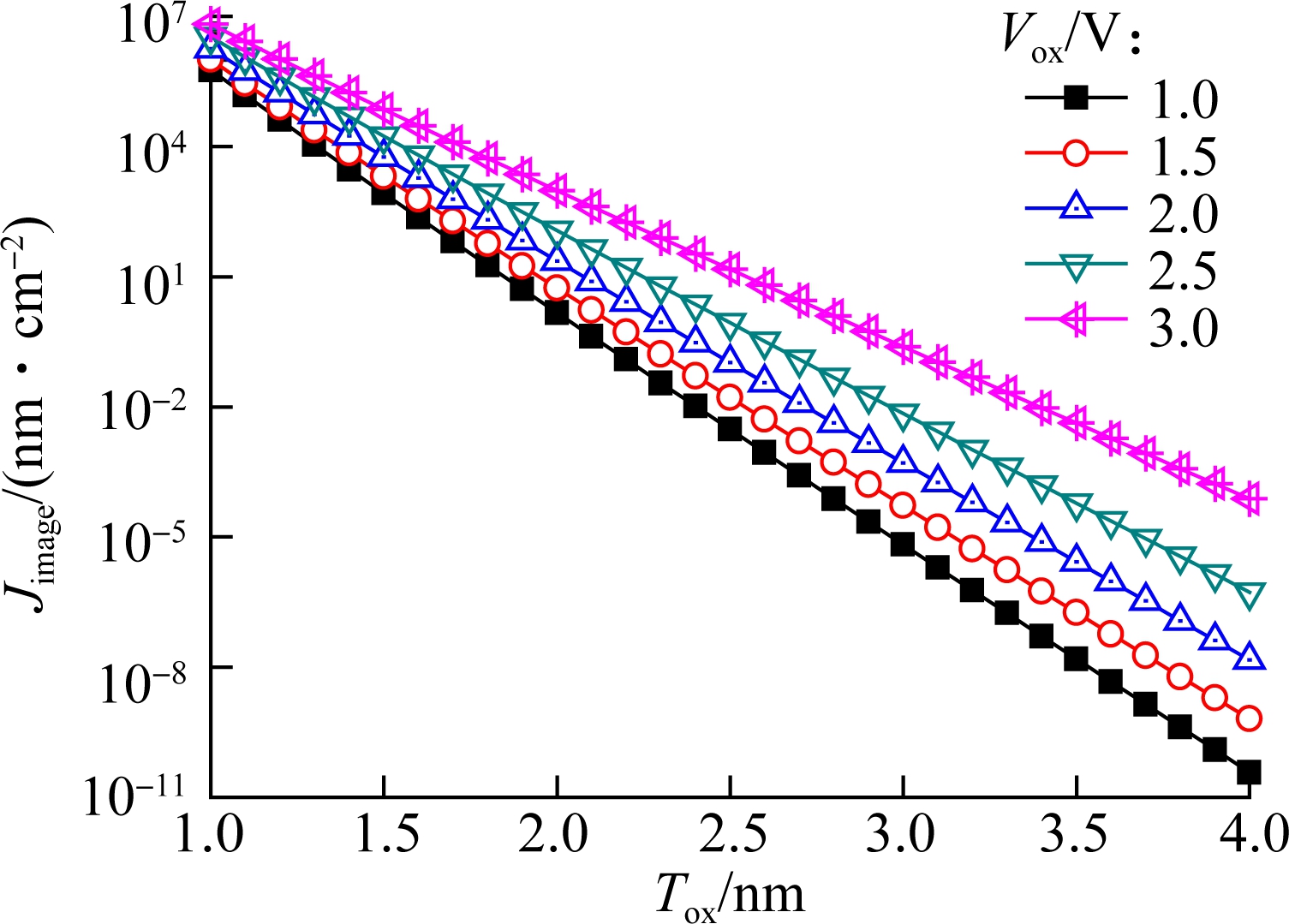
Fig.12 The tunneling current as a function of the oxide thickness with different applied voltage across gate oxide(φ=3.15 eV). (a) The FN tunneling current; (b) The direct tunneling current
Fig.12(b) shows the variation of the direct tunneling current under different gate voltages and oxide thicknesses, and the barrier reduction effect caused by the image potential is considered. It can be seen that the direct tunneling current reduces with the increase in the oxide thickness when the same gate voltage is applied. When the oxide thickness ranges from 1 to 4 nm, the direct tunneling current is reduced by 14 orders of magnitude when applied voltage is 2 V. The value is 11 when the applied voltage is 3 V. Under the same oxide thickness, the tunneling current increases with the increase in the gate voltage. It is also shown that the direct tunneling current cannot be ignored in a transistor with oxide thickness less than 3 nm.
These results indicate that the FN tunneling current is more dependent on the applied voltage across the gate oxide in the nano-scale transistor. We also conclude that when traditional methods such as increasing oxide thickness or reducing gate voltage are no longer useful for decreasing the leakage current, we can use the finite size effect to achieve this.
3 Conclusions
1) Both the bond length of the Si-Si and Si-O at the interface will be saturated when the interface size increases.
2) The finite size effect must be considered when the interface size is less than 2 nm. It can cause a change in the absorption spectrum of visible light. It implies that the absorption spectrum of visible light can be used as a tool to characterize the interface size.
3) When the device is nanoscale, the barrier height of Si/SiO2 decreases with the decrease of the interface size.
4) The tunneling current is significantly changed due to the finite size effect. It is well known that the existence of the transition region and image potential will cause a greater tunneling current. However, the increasing ratio will be weakened by the finite size effect.
5) This work can help us to clarify the impact of the finite size effect of the Si/SiO2 interface on tunneling current in nano-scale transistors. Not only can we better understand the characteristics of the interface, but also help to optimize the parameters of the next generation of nano-transistors in the future.
[1] Mudanai S, Fan Y Y, Ouyang Q, et al. Modeling of direct tunneling current through gate dielectric stacks[J].IEEE Transactions on Electron Devices, 2000, 47(10): 1851-1857. DOI:10.1109/16.870561.
[2] Feldman L C, Gusev E P, Garfunkel E. Ultrathin dielectrics in silicon microelectronics[M]//Fundamental Aspects of Ultrathin Dielectrics on Si-based Devices. Dordrecht: Springer Netherlands, 1998: 1-24. DOI:10.1007/978-94-011-5008-8_1.
[3] Hollinger G, Himpsel F J. Probing the transition layer at the SiO2-Si interface using core level photoemission[J]. Applied Physics Letters, 1984, 44(1): 93-95. DOI:10.1063/1.94565.
[4] Evans M H, Caussanel M, Schrimpf R D, et al. First-principles modeling of double-gate UTSOI MOSFETs[C]//IEEE International Electron Devices Meeting. Tempe, Arizon, USA, 2005:577-580. DOI:10.1109/iedm.2005.1609420.
[5] Hakala M H, Foster A S, Gavartin J L, et al. Interfacial oxide growth at silicon high-k oxide interfaces: First principles modeling of the Si-HfO2 interface[J]. Journal of Applied Physics, 2006, 100(4): 043708. DOI:10.1063/1.2259792.
[6] Green M L, Gusev E P, Degraeve R, et al. Ultrathin (<4 nm) SiO2 and Si-O-N gate dielectric layers for silicon microelectronics: Understanding the processing, structure, and physical and electrical limits[J]. Journal of Applied Physics, 2001, 90(5): 2057-2121. DOI:10.1063/1.1385803.
[7] Poindexter E H, Gerardi G J, Rueckel M E, et al. Electronic traps and Pb centers at the Si/SiO2 interface: Band-gap energy distribution[J]. Journal of Applied Physics, 1984, 56(10): 2844-2849. DOI:10.1063/1.333819.
[8] Muller D A, Sorsch T, Moccio S, et al. The electronic structure at the atomic scale of ultrathin gate oxides[J].Nature, 1999, 399(6738): 758-761. DOI:10.1038/21602.
[9] Watanabe T, Tatsumura K, Ohdomari I. SiO2/Si interface structure and its formation studied by large-scale molecular dynamics simulation[J]. Applied Surface Science, 2004, 237(1/2/3/4): 125-133. DOI:10.1016/j.apsusc.2004.06.044.
[10] Steinrück H G, Schiener A, Schindler T, et al. Nanoscale structure of Si/SiO2/organics interfaces[J]. ACS Nano, 2014, 8(12): 12676-12681. DOI:10.1021/nn5056223.
[11] Kova![]() evi
evi![]() G, Pivac B. Structure, defects, and strain in silicon-silicon oxide interfaces[J].Journal of Applied Physics, 2014, 115(4): 043531. DOI:10.1063/1.4862809.
G, Pivac B. Structure, defects, and strain in silicon-silicon oxide interfaces[J].Journal of Applied Physics, 2014, 115(4): 043531. DOI:10.1063/1.4862809.
[12] Bongiorno A, Pasquarello A. Atomistic structure of the Si(100)-SiO2 interface: A synthesis of experimental data[J]. Applied Physics Letters, 2003, 83(7): 1417-1419. DOI:10.1063/1.1604470.
[13] Diebold A C, Venables D, Chabal Y, et al. Characterization and production metrology of thin transistor gate oxide films[J]. Materials Science in Semiconductor Processing, 1999, 2(2): 103-147. DOI:10.1016/S1369-8001(99)00009-8.
[14] van Ginhoven R M, Hjalmarson H P. Atomistic simulation of Si/SiO2 interfaces[J]. Nuclear Instruments and Methods in Physics Research Section B: Beam Interactions with Materials and Atoms, 2007, 255(1): 183-187. DOI:10.1016/j.nimb.2006.11.022.
[15] Pasquarello A, Hybertsen M S, Car R. Structurally relaxed models of the Si(001)-SiO2 interface[J]. Applied Physics Letters, 1996, 68(5): 625-627. DOI:10.1063/1.116489.
[16] Yamasaki T, Kaneta C, Uchiyama T, et al. Geometric and electronic structures of SiO2/Si(001)interfaces[J]. Physical Review B, 2001, 63(11): 115314. DOI:10.1103/physrevb.63.115314.
[17] Tu Y H, Tersoff J. Structure and energetics of the Si-SiO2 interface[J]. Physical Review Letters, 2000, 84(19): 4393-4396. DOI:10.1103/physrevlett.84.4393.
[18] Kova![]() evi
evi![]() G, Pivac B. Modeling the interface between crystalline silicon and silicon oxide polymorphs[J].Physica Status Solidi, 2013, 210(4): 717-722. DOI:10.1002/pssa.201200447.
G, Pivac B. Modeling the interface between crystalline silicon and silicon oxide polymorphs[J].Physica Status Solidi, 2013, 210(4): 717-722. DOI:10.1002/pssa.201200447.
[19] Rani E, Ingale A, Phase D M, et al. Band gap tuning in Si-SiO2 nanocomposite: Interplay of confinement effect and surface/interface bonding[J]. Applied Surface Science, 2017, 425: 1089-1094. DOI:10.1016/j.apsusc.2017.07.133.
[20] Rani E, Ingale A A, Chaturvedi A, et al. Correlation of size and oxygen bonding at the interface of Si nanocrystal in Si-SiO2 nanocomposite: A Raman mapping study[J]. Journal of Raman Spectroscopy, 2016, 47(4): 457-467. DOI:10.1002/jrs.4832.
[21] Rani E, Ingale A A, Chaturvedi A, et al. Resonance Raman mapping as a tool to monitor and manipulate Si nanocrystals in Si-SiO2 nanocomposite[J]. Applied Physics Letters, 2015, 107(16): 163112. DOI:10.1063/1.4934664.
[22] Wen J L, Ma T B, Zhang W W, et al. Atomic insight into tribochemical wear mechanism of silicon at the Si/SiO2 interface in aqueous environment: Molecular dynamics simulations using ReaxFF reactive force field[J]. Applied Surface Science, 2016, 390: 216-223. DOI:10.1016/j.apsusc.2016.08.082.
[23] Ono T, Egami Y, Kutsuki K, et al. First-principles study of the electronic structures and dielectric properties of the Si/SiO2 interface[J]. Journal of Physics—Condensed Matter, 2001, 19(36): 365202.
[24] Corsetti F, Mostofi A A. A first-principles study of As doping at a disordered Si-SiO2 interface[J]. Journal of Physics: Condensed Matter, 2014, 26(5): 055002. DOI:10.1088/0953-8984/26/5/055002.
[25] Li H F, Guo Y Z, Robertson J, et al. Ab-initio simulations of higher Miller index Si: SiO2 interfaces for fin field effect transistor and nanowire transistors[J]. Journal of Applied Physics, 2016, 119(5): 054103. DOI:10.1063/1.4941272.
[26] Kim B H, Kim G, Park K, et al. Effects of suboxide layers on the electronic properties of Si(100)/SiO2 interfaces: Atomistic multi-scale approach[J]. Journal of Applied Physics, 2013, 113(7): 073705. DOI:10.1063/1.4791706.
[27] Ono T. First-principles study of leakage current through a Si/SiO2 interface[J]. Physical Review B, 2009, 79(19): 195326. DOI:10.1103/physrevb.79.195326.
[28] Markov S, Sushko P, Fiegna C, et al. Fromab initioproperties of the Si-SiO2 interface, to electrical characteristics of metal-oxide-semiconductor devices[J]. Journal of Physics: Conference Series, 2010, 242: 012010. DOI:10.1088/1742-6596/242/1/012010.
[29] Zafar S, Liu Q, Irene E A. Study of tunneling current oscillation dependence on SiO2 thickness and Si roughness at the Si/SiO2 interface[J]. Journal of Vacuum Science & Technology A: Vacuum, Surfaces, and Films, 1995, 13(1): 47-53. DOI:10.1116/1.579442.
[30] Sacconi F, di Carlo A, Lugli P, et al. Full band approach to tunneling in MOS structures[J].IEEE Transactions on Electron Devices, 2004, 51(5): 741-748. DOI:10.1109/ted.2004.826862.
[31] Yamada Y, Tsuchiya H, Ogawa M. A first principles study on tunneling current through Si/SiO2/Si structures[J]. Journal of Applied Physics, 2009, 105(8): 083702. DOI:10.1063/1.3106115.
[32] Herman F, Batra I P, Kasowski R V. The physics of SiO2 and its interfaces[M]. Oxford: Pergamon, 1978:333-338.
[33] Seino K, Bechstedt F. Effective density of states and carrier masses for Si/SiO2 superlattices from first principles[J]. Semiconductor Science and Technology, 2011, 26(1): 014024. DOI:10.1088/0268-1242/26/1/014024.
[34] Carrier P, Lewis L J, Dharma-Wardana M W C. Electron confinement and optical enhancement in Si/SiO2 superlattices[J]. Physical Review B, 2001, 64(19): 195330. DOI:10.1103/physrevb.64.195330.
[35] Seino K, Wagner J M, Bechstedt F. Quasiparticle effect on electron confinement in Si SiO2 quantum-well structures[J]. Applied Physics Letters, 2007, 90(25): 253109. DOI:10.1063/1.2750526.
[36] Zhu H W, Liu Y S, Mao L F, et al. Theoretical study of the SiO2/Si interface and its effect on energy band profile and MOSFET gate tunneling current[J]. Journal of Semiconductors, 2010, 31(8): 082003. DOI:10.1088/1674-4926/31/8/082003.
[37] Segall M D, Lindan P J D, Probert M J, et al. First-principles simulation: Ideas, illustrations and the CASTEP code[J].Journal of Physics: Condensed Matter, 2002, 14(11): 2717-2744. DOI:10.1088/0953-8984/14/11/301.
[38] Perdew J P, Burke K, Ernzerhof M. Generalized gradient approximation made simple[J].Physical Review Letters, 1996, 77(18): 3865. DOI:10.1103/physrevlett.77.3865.
[39] Jie W J, Chen X, Li D, et al. Layer-dependent nonlinear optical properties and stability of non-centrosymmetric modification in few-layer GaSe sheets[J]. Angewandte Chemie (International Edition in English), 2015, 54(4): 1185-1189. DOI:10.1002/anie.201409837.
[40] Niedfeldt K, Carter E A, Nordlander P. First principles resonance widths for Li near an Al(001) surface: Predictions of scattered ion neutralization probabilities[J].The Journal of Chemical Physics, 2004, 121(8): 3751-3755. DOI:10.1063/1.1777218.
[41] Lu Z H, Lockwood D J, Baribeau J M. Quantum confinement and light emission in SiO2/Si superlattices[J]. Nature, 1995, 378(6554): 258-260. DOI:10.1038/378258a0.
[42] Chen H X, Shi D N, Qi J S, et al. The stability and electronic properties of wurtzite and zinc-blende ZnS nanowires[J].Physics Letters A, 2009, 373(3): 371-375. DOI:10.1016/j.physleta.2008.11.060.
[43] van de Walle C G, Martin R M. Theoretical study of band offsets at semiconductor interfaces[J].Physical Review B, 1987, 35(15): 8154. DOI:10.1103/physrevb.35.8154.
[44] Yamashita Y,Yamamoto S,Mukai K. Direct observation of site-specific valence electronic structure at the SiO2 Si interface[J]. Physical Review B, 2006, 73(4): 45336.
[45] Alkauskas A, Broqvist P, Devynck F, et al. Band offsets at semiconductor-oxide interfaces from hybrid density-functional calculations[J]. Physical Review Letters, 2008, 101(10): 106802. DOI:10.1103/physrevlett.101.106802.
[46] Kimura K, Nakajima K. Compositional transition layer in SiO2/Si interface observed by high-resolution RBS[J]. Applied Surface Science, 2003, 216(1/2/3/4): 283-286. DOI:10.1016/s0169-4332(03)00386-6.
[47] Ando Y, Itoh T. Calculation of transmission tunneling current across arbitrary potential barriers[J].Journal of Applied Physics, 1987, 61(4): 1497-1502. DOI:10.1063/1.338082.
[48] Mao L F, Tan C H, Xu M Z. The effect of image potential on electron transmission and electric current in the direct tunneling regime of ultra-thin MOS structures[J]. Microelectronics Reliability, 2001, 41(6): 927-931. DOI:10.1016/s0026-2714(01)00037-3.
[49] Mao L F, Tan C H, Xu M Z. Estimate of width of transition region of barrier for thin film insulator MOS structure using Fowler-Nordheim tunneling current[J]. Chinese Journal of Semiconductors, 2001, 22(2): 228-233.(in Chinese)
[50] Jeppson K O. Influence of the channel width on the threshold voltage modulation in m.o.s.f.e.t.s[J].Electronics Letters, 1975, 11(14): 297-299. DOI:10.1049/el:19750225.
[51] Fuse G, Fukumoto M, Shinohara A, et al. A new isolation method with boron-implanted sidewalls for controlling narrow-width effect[J].IEEE Transactions on Electron Devices, 1987, 34(2): 356-360. DOI:10.1109/t-ed.1987.22930.
[52] Yeo Y C, Lu Q, Lee W C, et al. Direct tunneling gate leakage current in transistors with ultrathin silicon nitride gate dielectric[J].IEEE Electron Device Letters, 2000, 21(11): 540-542. DOI:10.1109/55.877204.