With the rapid development of electronic information technology, the electronic countermeasure (ECM) will be faced with demanding requirements in terms of sensitivity, wide instantaneous bandwidth, anti-interference ability and portability. Therefore, as the core part of an ECM system, high-performance, miniaturized mixing components have become one of the important research directions. With the development of bulk silicon micromachining technology, the use of new technologies such as the micro-electro-mechanical system(MEMS) and though silicon via(TSV) to develop miniaturized transceiver systems has become a new option[1-7]. With the silicon-based adapter board technology, it is possible to integrate passive and active devices (GaAs, CMOS chips, etc.) on a single high-resistance silicon substrate[8]. Combining SIP, SOP, POP and other 3D integration technologies, the SWP performance of the ECM system will be further maximized[9-11].
In this paper, using silicon-based adapter board technology, the broadband miniaturized 3D heterogeneous integrated chips covering the Ku frequency band are realized, and the silicon-based interdigital band filter is optimized. Using TSV and wafer-level gold-gold bonding and other 3D integration technology, the integrated design of the microwave chip and passive filter is implemented. Then, a mixing component is assembled by the proposed mixing multi-function chip and frequency multiplier multi-function chip and can better meet the needs of miniaturized applications.
1 Overall Scheme
The block diagram of the broadband mixing component is shown in Fig.1. The key point of the design is to optimize specifications such as in-band spurs without worsening the noise figure (NF). The quality of the NF depends on the gain of the RF circuit. In other words, a higher front-end circuit gain helps to improve the NF of the mixing component. The spur performance mainly depends on the mixing intermodulation suppression capability and the relative bandwidth of the RF/IF. In order to ensure that the spur after the two conversions does not fall within the signal bandwidth, the design adopts an extremely high frequency local oscillator (LO) mixing scheme and double conversion, in which the frequency of the first conversion LO signal is close to 60 GHz. Meanwhile, to ensure the quality factor of the LO signal, the LO generating circuit uses a frequency multiplier multi-function chip circuit based on a triple frequency multiplier. This paper mainly focuses on the miniaturized integration of the mixing multi-function chip and frequency multiplier multi-function chip with high performance.
As shown in Fig.1, the mixing multi-function chip integrates functional circuits such as band-pass filter, mixer, attenuator, amplifier, and adopts double balanced mixing circuits to achieve a general design of the two-stage mixing units, while the frequency multiplier chip mainly integrates functional circuits such as the frequency tripler, band-pass filter and amplifier to reduce the design difficulty of millimeter wave LO and the risk of electromagnetic leakage of extremely high frequency signals. Both of the multi-function chips use advanced 3D heterogeneous integration technology to achieve miniaturized integration.
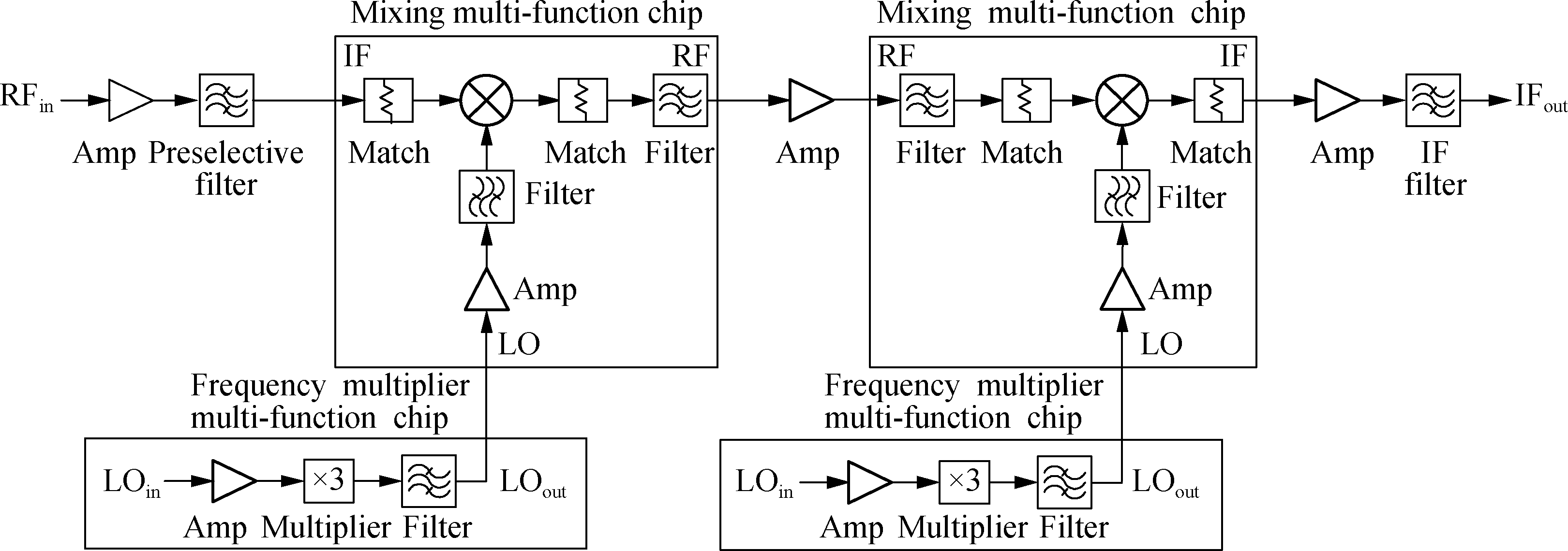
Fig.1 Block diagram of the broadband mixing component
2 Design of the 3D Heterogeneous Integrated Chips
Aimed at the integration of the above two multi-function chips, this paper proposes a silicon-based 3D stack structure model. As shown in Fig.2, there are four silicon-based layers. The first layer is the grounding base layer; the core monolithic integrated microwave chip (MMIC) is embedded in the second layer of the silicon cavity; the silicon-based filter is integrated with the high-resistance silicon substrate in the third layer. Each layer adopts TSV technology to realize signal interconnection. Four layers of high-resistance silicon substrate stack packaging are implemented based on the wafer-level gold-gold bonding process.

Fig.2 Model of silicon-based multi-function chip
2.1 Design and simulation of the mixing multi-function chip
The mixing multi-function chip mainly processes frequency conversion on the pre-stage RF signal of the downconverter, and mainly integrates the functions of amplification, frequency conversion, LO and IF signal filtering on the chip. The key problem of the mixing multi-function chip is how to design a suitable filter to complete the high-Q transmission of RF and LO signals.
The filtering function of RF and LO signal is realized by the silicon-based interdigital strip filter structure. The simulation model of the RF silicon-based filter is shown in Fig.3, and the simulation results are shown in Fig.4. It can be seen that the filter suppression is greater than 20 dB at 39 and 45 GHz, and the suppression is greater than 70 dB at 34.5 and 49.5 GHz, which meets the basic design requirements.
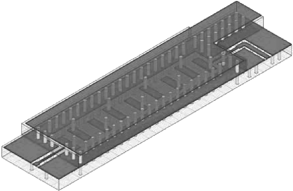
Fig.3 Simulation model diagram of RF silicon-based filter
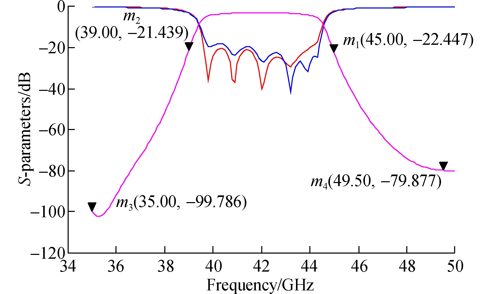
Fig.4 Simulation results of RF silicon-based filter
Considering the loss and matching performance of microstrip transmission for the 60 GHz LO signal in the packaged chip, a substrate integrated waveguide (SIW) transmission structure that is more suitable for millimeter wave transmission is employed to ensure the quality of RF signal transmission. In addition, in order to facilitate the bonding connection between the internal chip and the microstrip structure, a coplanar waveguide (CPWG) to SIW plane transmission structure is applied, and more dense ground vias are used around the transmission structure to ensure isolation. The transmission structure design and simulation results of CPWG to SIW are shown in Figs.5 and 6.
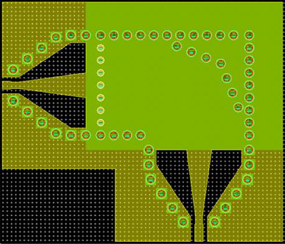
Fig.5 The transmission structure of CPWG to SIW
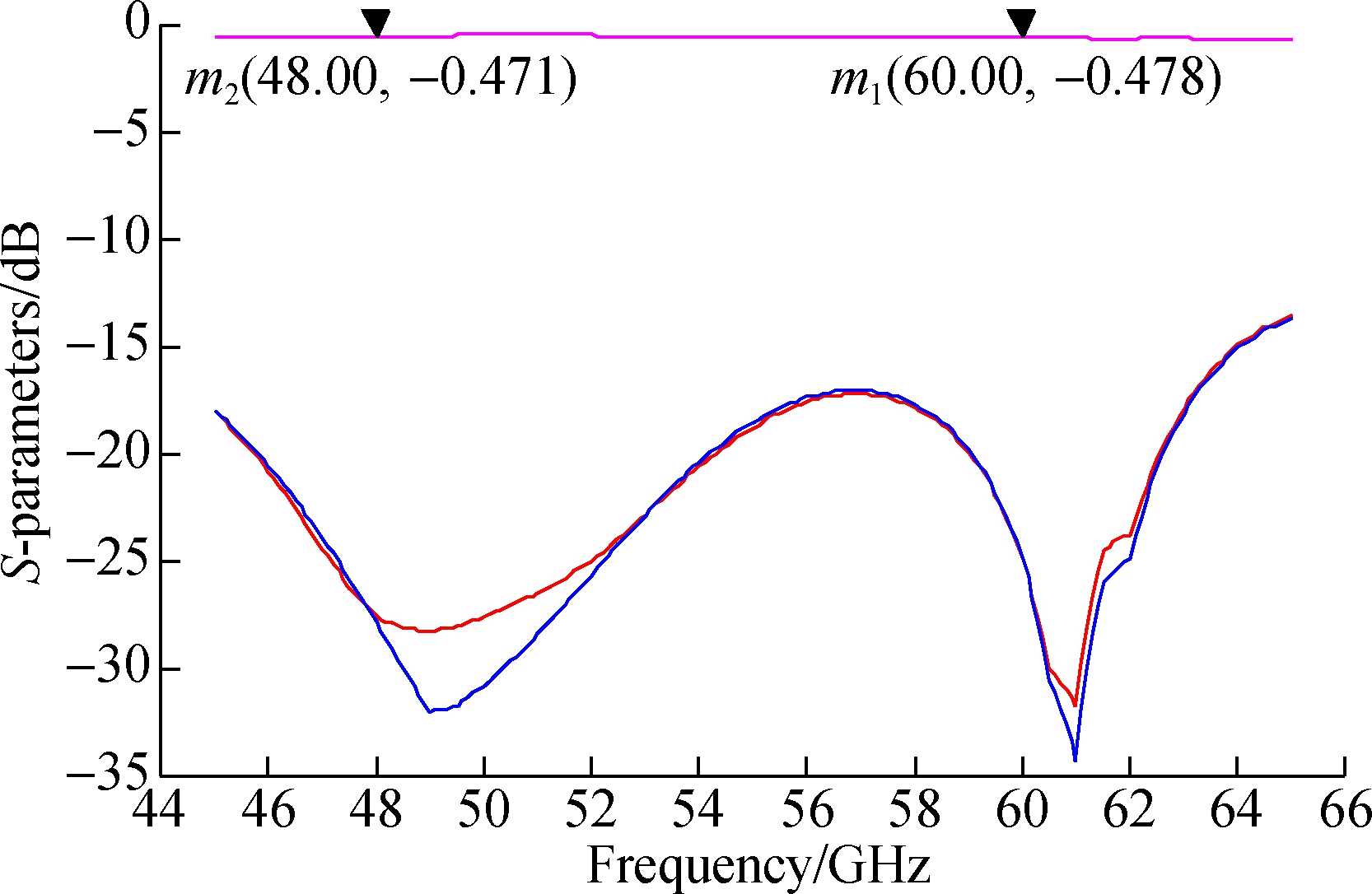
Fig.6 The simulation results of CPWG to SIW
It can be seen that the 90° transmission structure from CPWG to SIW has a VSWR of less than 1.5, a loss of less than 0.5 dB, and a flatness of less than 0.1 dB in the entire frequency band, which shows excellent performance.
2.2 Design and simulation of frequency multiplier multi-function chip
The frequency multiplier multi-function chip integrates amplifier, attenuator, frequency tripler and filter. In order to reduce the transmission loss of the high frequency millimeter wave signal and solve the electromagnetic compatibility problem of the signal in the frequency conversion component, the frequency multiplier multi-function chip is used to triple the LO signal in the Ku band to obtain the extremely high frequency LO signal required for mixing. According to the mixing spurious index, the suppression of the fundamental wave (1/3×LO) and the second harmonic (2/3×LO) of the LO signal must be greater than 90 dBc.
This work is based on a two-stage silicon-based stripline filter to achieve a high rejection design of the LO filter, and the two-stage filters are placed in different packaged chips (multiplication and mixing multi-function chips) to reduce their mutual influence. The single-stage filter structure is shown in Fig.7, and the simulation results are shown in Fig.8. It can be seen that the suppression of the single-stage filter is better than 55 dBc at 40 GHz, and the cascade suppression of the two-stage filter is better than 100 dBc. In addition, the LO frequency of the second-stage mixing of the down-converter described in this paper is set between 48 and 60 GHz. Along with the filtering structure, the same frequency multiplier multi-function chip can be used for the two-stage mixer.
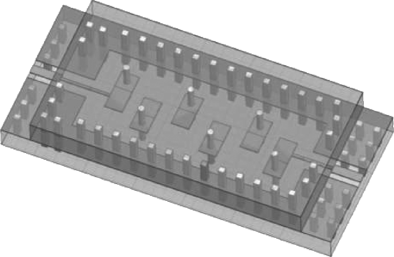
Fig.7 LO silicon-based filter simulation model diagram
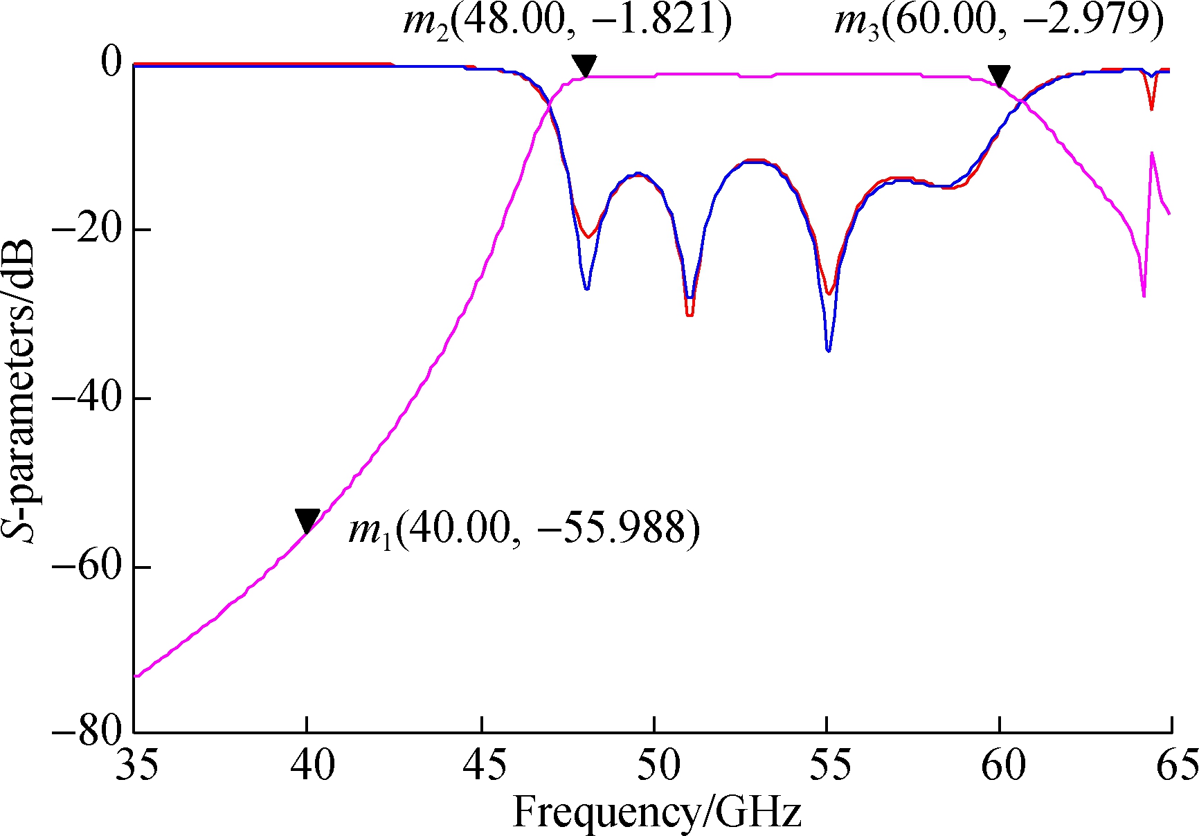
Fig.8 LO silicon-based filter simulation results
3 Implementation Results
3.1 Test results of the multi-function chips
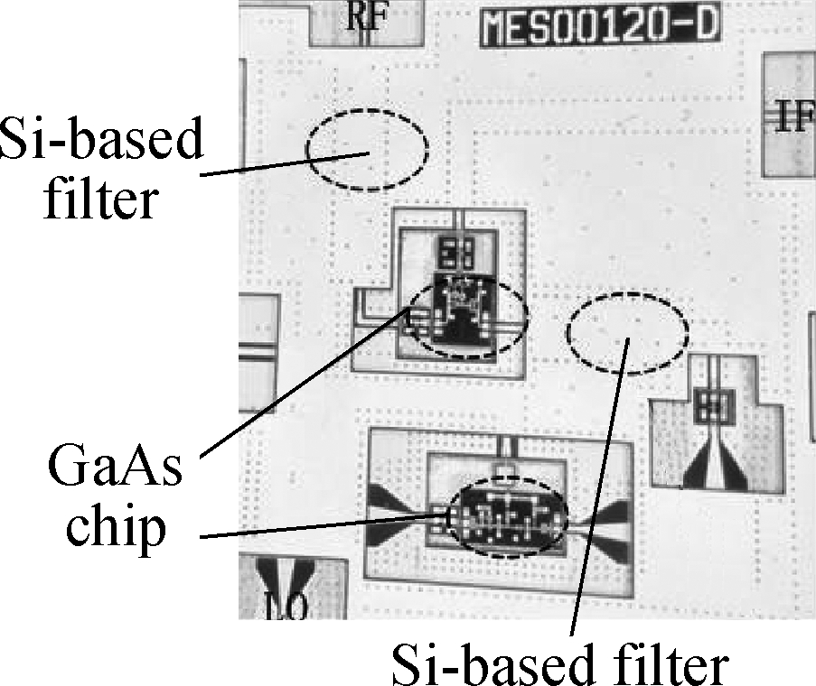
The cavity and inter-connect line of the silicon-based adapter board are designed with AutoCAD. The mixing multi-function chip and the frequency multiplier multi-function chip without a package cover is shown in Fig.9. A large number of grounding vias are set around the cavity of the MMIC chip and the signal transmission line to ensure grounding continuity. Meanwhile, this design minimizes the mutual interference of microwave signals inside and outside the cavity and improves the electrom-agnetic compatibility of the multi-function chip.
(a) 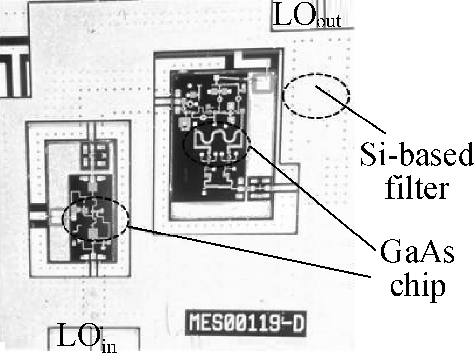 (b)
(b)
Fig.9 The physical picture of the multi-function chips. (a) The mixing multi-function chip; (b)The frequency multiplier multi-function chip
The test results of the mixing multi-function chip and the frequency multiplier multi-function chip are shown in Tab.1 and Tab.2.
Tab.1 Test results of the mixing multi-function chip
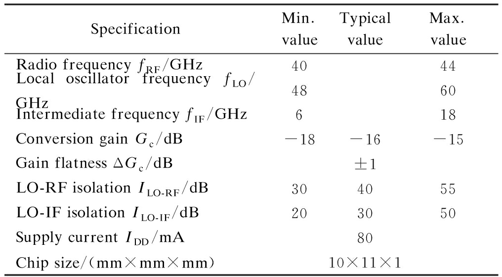
SpecificationMin. valueTypical valueMax. valueRadio frequency fRF/GHz4044Local oscillator frequency fLO/GHz4860Intermediate frequency fIF/GHz618Conversion gain Gc/dB-18-16-15Gain flatness ΔGc/dB±1LO-RF isolation ILO-RF/dB304055LO-IF isolation ILO-IF/dB203050Supply current IDD/mA80Chip size/(mm×mm×mm)10×11×1
Tab.2 Test results of the frequency multiplier multi-function chip
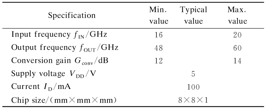
SpecificationMin. valueTypical valueMax. valueInput frequency fIN/GHz1620Output frequency fOUT/GHz4860Conversion gain Gconv/dB1214Supply voltage VDD/V5Current ID/mA100Chip size/(mm×mm×mm)8×8×1
3.2 Test results of the broadband mixing component
As shown in Fig.1, the mixing multi-function chip and the frequency multiplier multi-function chip are cascaded to form the broadband mixing component. The inter-stage also includes a pre-selector filter, an amplifier and an IF filter. The photo of the fully assembled mixing component is shown in Fig.10.
A signal source is used to generate appropriate RF signals and LO signals to test the spur and gain from the output IF signal, as shown in Figs.11-13. The overall spur is better than -50 dBc and the gain is better than 15 dB.
3.3 Comparison and analysis of test results
The comparison of the multi-function chip test results is shown in Tab.3. It can be found that this paper presents 3D heterogeneous integrated wideband RF chips based on silicon-based adapter board technology with complex integration, a compact size and wider bandwidth.
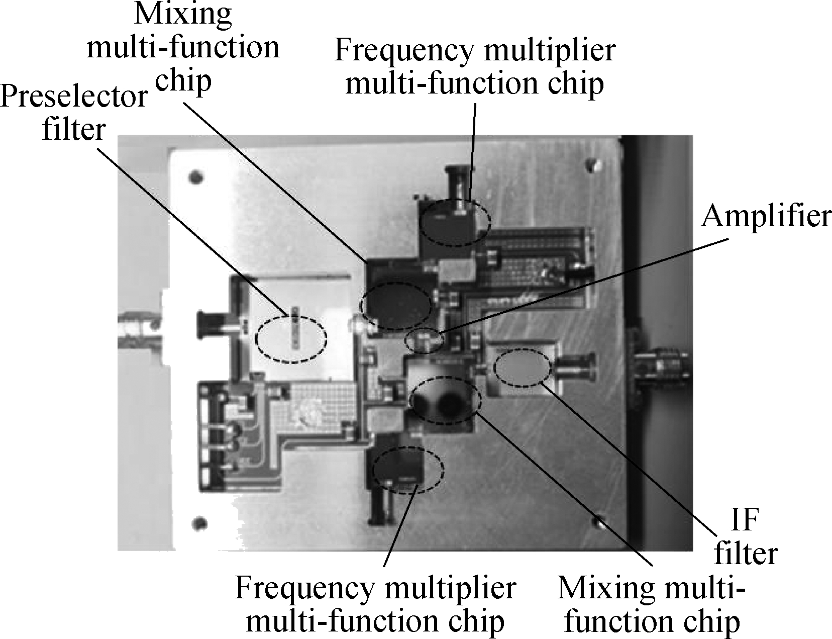
Fig.10 Photo of the cascade broadband mixing component
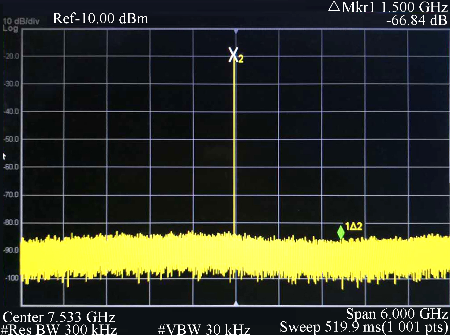
Fig.11 Spur spectrum test results
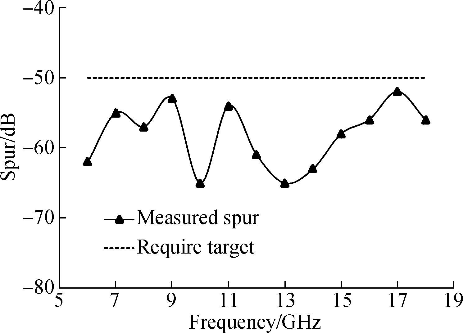
Fig.12 Measured spur
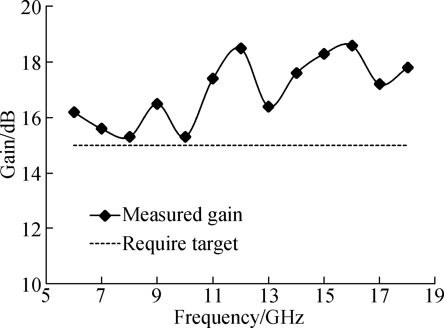
Fig.13 Measured gain
Tab.3 Comparison of the multi-function chips test results

ItemTransceiver module[2]Transceiver SiP module[11]This paperMixing multi-function chipFrequency multiplier multi-function chipIntegrationTransceiver and antennasRF front-end, ADC and DACBand-pass filter, mixer, attenuator, and amplifierFrequency-tripler, band-pass filter and amplifierFrequency/GHz60S and P band40 to 4448 to 60Bandwith/GHz1.76412Size/(mm×mm×mm)6.5×6.5×0.638×40×410×11×18×8×1TechnologyTSV,ball grid arrayBall grid arrayTSV,gold-gold bondingTSV, gold-gold bonding
4 Conclusion
1) This paper adopted the silicon-based adapter board technology and implemented two multi-function chips. The mixing multi-function chip has a chip size of 10 mm × 11 mm × 1 mm. The RF frequency is 40-44 GHz, the IF covers the Ku band with greater than a 4 GHz instantaneous IF bandwidth. The frequency multiplier multi-function chip works in the 16-20 GHz frequency band, of which fundamental suppression is better than 50 dB and the second harmonic suppression is better than 40 dB, with a chip size of 8 mm×8 mm×1 mm.
2) The designed mixing multi-function chip and frequency multiplier multi-function chip are cascaded to form a broadband mixing component, which shows good test performance and can meet application requirements.
3) The proposed architecture combines 3D integration technologies such as SIP, SOP and POP to finally achieve a great improvement of the SWP to facilitate a broadband RF front-end system with excellent overall performances.
[1] Pares G, Jean-Philippe M, Edouard D, et al. Highly compact RF transceiver module using high resistive silicon interposer with embedded inductors and heterogeneous dies integration[C]//2019 IEEE 69th Electronic Components and Technology Conference (ECTC). Las Vegas, NV, USA, 2019: 1279-1286. DOI:10.1109/ECTC.2019.00198.
[2] Bouayadi O E, Dussopt L, Lamy Y, et al. Silicon interposer: A versatile platform towards full-3D integration of wireless systems at millimeter-wave frequencies[C]//2015 IEEE 65th Electronic Components and Technology Conference (ECTC). San Diego, CA, USA, 2015: 973-980. DOI:10.1109/ECTC.2015.7159713.
[3] Liang H M, Liu S, Xiong B. TSV-free vertical interconnection technology using Au-Si eutectic bonding for MEMS wafer-level packaging[C]//2019 20th International Conference on Solid-State Sensors, Actuators and Microsystems & Eurosensors ⅩⅩⅩⅢ. Berlin, Germany, 2019: 1666-1669. DOI:10.1109/TRANSDUCERS.2019.8808412.
[4] Zhang M, Yang J, He Y R, et al. Research on a 3D encapsulation technique for capacitive MEMS sensors based on through silicon via[J].Sensors, 2018, 19(1): E93. DOI:10.3390/s19010093.
[5] Li N N, Xing C Y. Development of inertial micro-system packaging and integration technology[J]. Navigation and Control, 2018, 17(6): 28-34. DOI:10.3969/j.issn.1674-5558.2018.06.005 .(in Chinese)
[6] Sun L, Chen M H, Zhang L, et al. Recent progress in SLID bonding in novel 3D-IC technologies[J].Journal of Alloys and Compounds, 2020, 818: 152825. DOI:10.1016/j.jallcom.2019.152825.
[7] Wang Q, Liu Z, Jiang J, et al. A new cellular-based redundant TSV structure for clustered faults[J]. IEEE Transactions on Very Large Scale Integration Systems, 2019, 27(2): 458-467. DOI:10.1109/TVLSI.2018.2876906.
[8] Huang M, Zhu J, Shi G X. Silicon interposer combined with integrated passive devices for micro/millimeter wave application[J]. Equipment for Electronic Products Manufacturing, 2017, 46(4): 20-23.(in Chinese)
[9] Zhao Y Z, Wang S D. A novel 3D T/R module with MEMS technology[C]//2016 International Conference on Integrated Circuits and Microsystems (ICICM). Chengdu, China, 2016: 286-289. DOI:10.1109/ICAM.2016.7813609.
[10] Tummala R R. 3D system package architecture as alternative to 3D stacking of ICs with TSV at system level[C]//2017 IEEE International Electron Devices Meeting (IEDM). San Francisco, CA, USA, 2017: 3.4.1-3.4.3. DOI:10.1109/IEDM.2017.8268319.
[11] Liu J F, Wang B, Zhou Y, et al. Design and implementation of a dual-band RF SiP module based on package-on-package technology[C]//2018 International Conference on Microwave and Millimeter Wave Technology (ICMMT). Chengdu, China, 2018: 1-3. DOI:10.1109/ICMMT.2018.8563973.