With the gradual popularization of 5G and the growing demand for autonomous driving systems, buck converters with high power density and low noise have been widely used. At present, the radar systems in 5G communication systems and autonomous driving systems not only require large currents but also place high demands on the ripple and noise of the power supply. Noise can be reduced when a secondary filter is cascaded at the output of a buck converter.Small-signal models have been analyzed, and a guideline for the design of secondary filters has been proposed. However, a stability analysis of different secondary filters based on loop control has yet to be performed[1-2]. A fourth-order low-pass filter composed of equivalent inductance and external capacitance can be effectively used by designing printed circuit board (PCB) traces, but it can only filter out high-frequency noise [3]. On the basis of a delta-sigma modulator with a loop filter, noise can be successfully shaped, but the output ripple is still as high as 19 mV[4]. With the progress of semiconductor technology, the power supply voltage of core processors has decreased while current demand has increased. Hence, the accuracy requirements for the power supply have also increased. In the case of a large increase in load current transient response and slew rate, most processors currently require the total accuracy of the power supply to be within ±5% (static and dynamic). To improve dynamic system performance, studies have adopted AVP and have widely discussed the methods for its implementation. In addition to the output voltage feedback path, an additional AVP filter can be introduced to adjust the error amplifier reference in real-time, but it can easily result in output oscillation when the load jumps, and no specific analysis of loop stability has been conducted[5]. Adjusting load line resistance on the fly can effectively improve dynamic performance and direct current (DC) accuracy; however, doing so requires additional control circuits, such as transconductance amplifiers and voltage-controlled current sources, which also increase the complexity and cost of control[6-8]. A buck converter with digital control can eliminate current sampling through the current sensorless AVP mechanism, but it requires a high-precision analog-to-digital converter to obtain current information; hence, the complexity and cost of system development increase[9-10]. To reduce the effective value of noise integration in the frequency range of 10 to 1×10⁵ Hz and optimize the noise spectrum density at a specific frequency while meeting the required output voltage dynamic performance and specific accuracy, the current study proposes a buck converter on the basis of a secondary filter and AVP control. Relative to the traditional buck converter, the proposed buck converter does not increase the complexity and cost of the control method, and it can effectively reduce the output voltage noise and enhance dynamic response performance. Meanwhile, a small-signal model of the control method is also presented, along with an analysis of loop stability and control circuit parameters. The feasibility of the scheme is verified by the modeling calculation and experimental results.
1 Buck Converter with Secondary Filter
1.1 System architecture
To reduce the output noise of a buck converter, a second-stage filter can be cascaded after the output LC filter, which can substantially reduce the noise generated by the switching frequency and higher harmonics. However, adding a second-stage filter affects loop stability and DC regulation. As shown in Fig.1, the remote feedback method uses the output of the second-stage filter as a feedback node, which has good DC regulation performance. However, the loop bandwidth is too small and thus directly affects the stability and dynamic response performance. Another approach is the local feedback method, which uses the input of the second-stage filter as the feedback node. Although this method can improve the loop bandwidth and dynamic response performance, the impedance of the PCB trace and the DCR of the second-stage inductor causes a voltage drop with the load, thereby affecting DC regulation.

To improve the DC regulation and loop stability, this study proposes a hybrid feedback control method (see Fig.2). The hybrid feedback control method not only guarantees DC regulation with the remote feedback method but also improves loop stability and dynamic response performance by adding high-frequency feedback paths CF and RF.

Fig.2 Buck with secondary filter and hybrid feedback
1.2 Small-signal analysis
In this study, a small-signal model of the secondary filter of the buck converter is derived on the basis of the peak current mode buck converter to analyze the influence of the hybrid feedback method on stability and to design a high-frequency feedback path. The control loop diagram is shown in Fig.3. GF1 is the high-frequency feedback path transfer function from local output V1 to VFB. GF2 is the low-frequency feedback path transfer function from remote output V2 to VFB. Gv1d and Gv2d are the transfer functions of the output voltages V1 and V2 to the duty cycle, respectively.
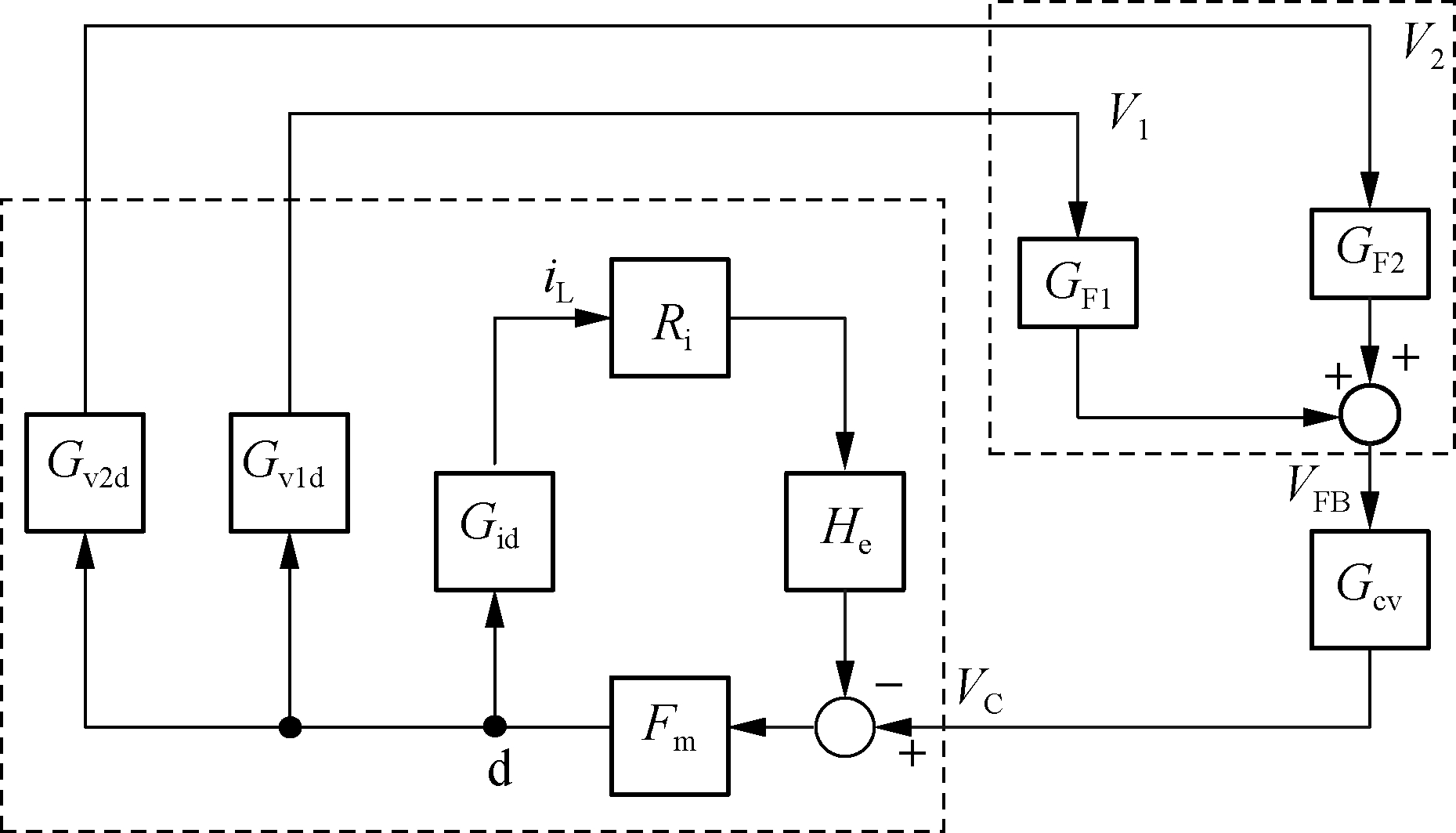
Fig.3 Small-signal model of peak current mode buck converter with secondary filter and hybrid feedback
The output impedance Z1 of V1 is
(1)
The output impedance Z2 of V2 is
(2)
The transfer function of local output V1 to the inductor current is
(3)
The transfer function of remote output V2 to the inductor current is
(4)
The transfer function of the inductor current to the duty cycle is
(5)
The transfer functions of the output voltages V1 and V2 to the duty cycle are given, respectively, as
(6)
(7)
The transfer function of the current inner loop is
(8)
Thus, the transfer functions of the output voltages V1 and V2 to the control node VC can be respectively derived as
(9)
(10)
where Gv1c and Gv2c are the control-to-output (V1 and V2, respectively) transfer functions.
Therefore, the loop gain is
(11)
Here, GCV is the error amplifier compensator transfer function, and K is the ratio of GV1C and GV2C.
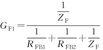
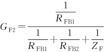
GFB=GF2+GF1K
(13)
(14)
(15)
(16)
(17)
The feedback transfer function GFB has one conjugate zero pair fZ, and the control transfer Gv2c has one conjugate pole pair fP, as shown in the following equations:
(18)
(19)
The conjugate zero pair is made to cancel the conjugate pol part to reduce the impact on the loop control. RF can be expressed as
(20)
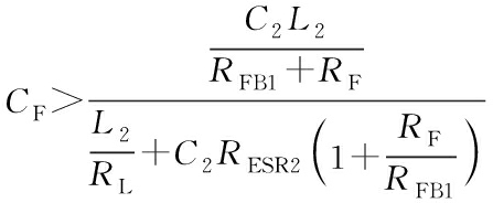
Fig.4 shows the gain and phase of GFB. If the value of CF is too small, then the zero pair in GFB moves to the right half plane, thus causing a 180° phase delay and instability. To keep the zero-point pair on the left half plane, the following requirement needs to be met:
(21)
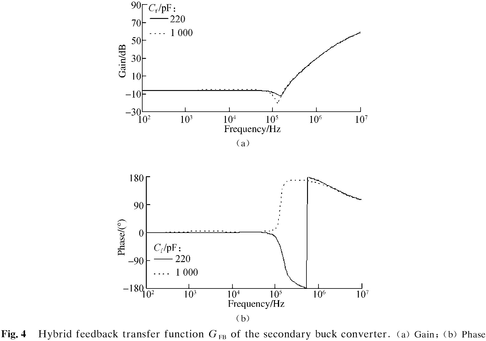
Fig.5 shows the gain and phase of the loop gain T. If the value of CF is too small, then the zero pair in GFB moves to the right half plane, thereby causing a 180° phase delay and instability.
2 Buck Converter with AVP Control
To reduce the fluctuation of the output voltage when the load jumps, this study proposes a low-cost and easy-to-implement AVP control method (see Fig.6). By adding a load line resistor between the output voltage feedback node VFB and the output of the error amplifier, the low-frequency gain of the loop is reduced to increase
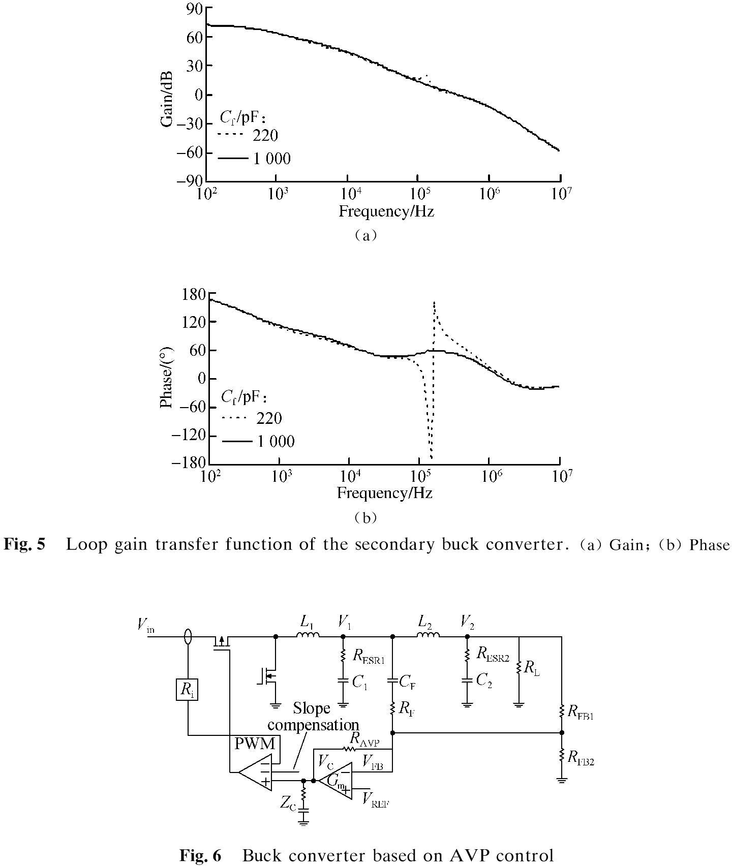
the load regulation of the output voltage and thereby optimize the dynamic response of the output voltage.
The AVP control method is analyzed using a small-signal model that obtains the loop transfer function and its influence on loop stability. AVP control differs from the conventional control loop in terms of the error amplifier. In this work, the equivalent circuit is altered to facilitate the analysis(see Fig.7).
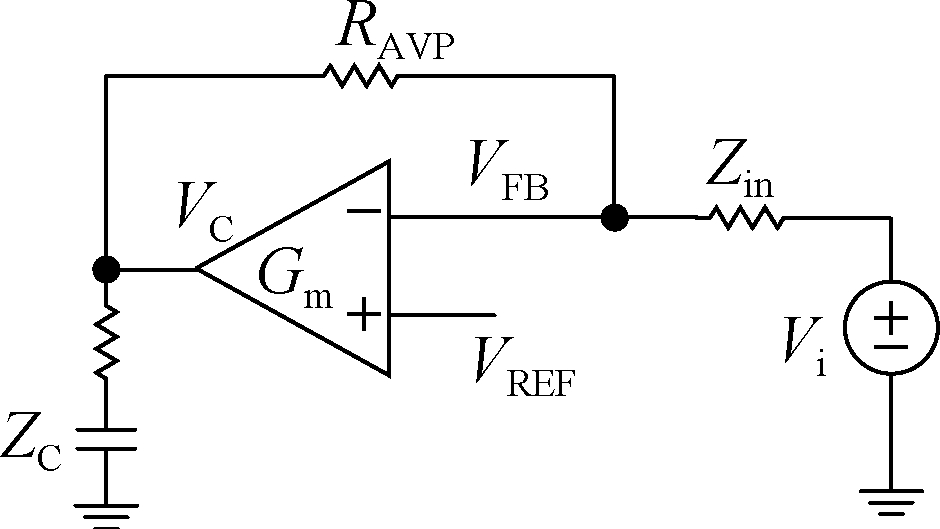
Fig.7 Equivalent control diagram of error amplifier with AVP
The following formulas can be obtained by analyzing the virtual short and virtual break of the amplifier.
(22)
(23)
Here, Zin is the equivalent input impedance of the amplifier.
(24)
The input to the control transfer function of the error amplifier can be derived as
(25)
(26)
Eq.(26) is substituted into Eq. (25), and the output to the control transfer function is
(27)
The loop gain of the AVP buck converter is
(28)
where GVC is the control for the output transfer function given as
(29)
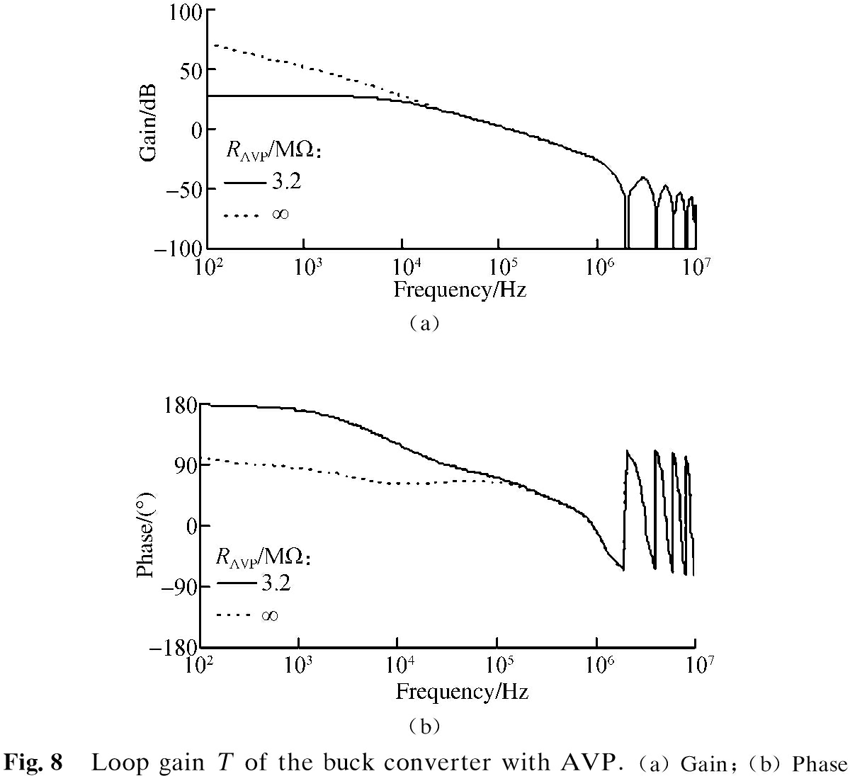
From the perspective of amplitude frequency characteristics (see Fig.8), the control loop transfer function only reduces the low-frequency gain without affecting the loop bandwidth. Similarly, the phase frequency characteristics only change the low-frequency phase without affecting the phase margin of the loop. It facilitates the design of the compensator without increasing the complexity of the control loop and the system cost.
The selection of the value of RAVP is discussed herein. Assuming that the system requires ΔVO_MAX as the output voltage accuracy specification, the output deviation ΔVO_TR is caused by the dynamic load without RAVP. The load regulation changes ΔVO_LR caused by RAVP can be obtained by
ΔVO_MAX=ΔVO_TR-ΔVO_LR
(30)
The closed-loop output impedance is
(31)
The low frequency gain of the loop gain is
(32)
The load regulation can be calculated by
(33)
Thus, the value of RAVP can be derived as
(34)
3 Experimental Results
The prototype is based on a 10 A, 8 MHz buck converter with a secondary filter and AVP control for experimental analysis. The prototype specifications are listed in Tab.1.
Tab.1 Prototype specifications

ParameterValueVin/V3.3VO/V1.0Inductor/nH 100Output capacitor/μF47Secondary filter/nH220Hybrid feedforward/kΩ15Error amplifier gain/μS800Compensation resistor/kΩ30Compensation capacitor/pF20AVP resistor/MΩ3.2
The results of the noise spectral density are shown in Fig.9(a), and the integrated noise of the specific frequency range can be obtained accordingly. The output noise can be suppressed, especially when the frequency exceeds 1 MHz, that is sensitive for the downstream devices. Fig.9(b) shows a 30 mV peak-to-peak output ripple without the secondary filter and a small 1.7 mV peak-to-peak output ripple with the secondary filter.
The comparison of the dynamic response results demonstrates that AVP control effectively improves the output voltage dynamic response (see Fig.10). The experimental results show that load regulation increases by 3%, but the output deviation caused by the load step improves by 2%. Therefore, the output voltage accuracy (static and dynamic) meets the 5% accuracy requirement of downstream devices. In other words, the buck converter requires minimal output capacitance and therefore reduces system cost.
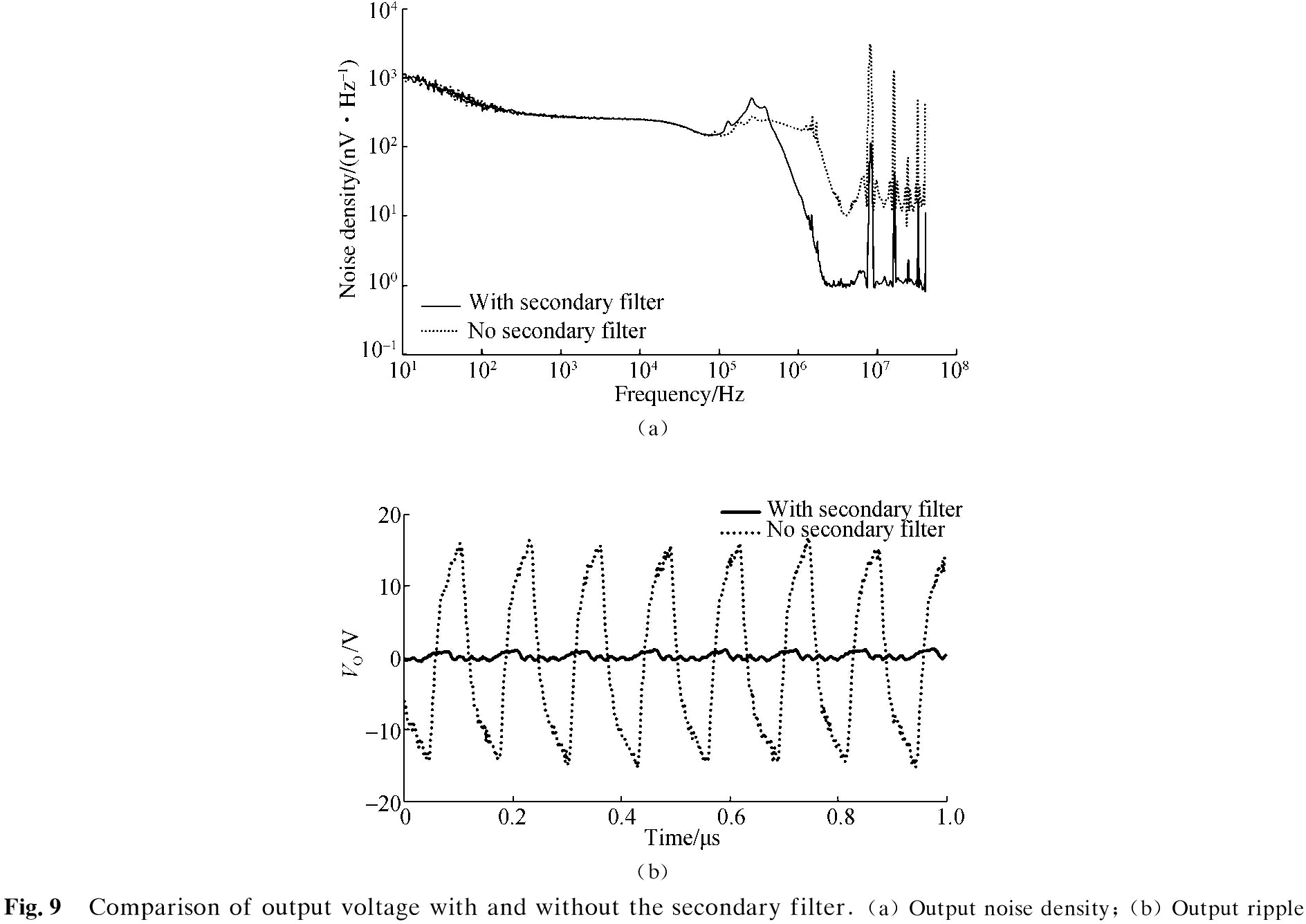
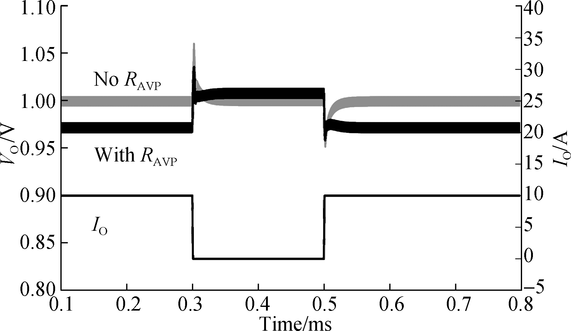
Fig.10 Comparison of load transient with and without RAVP
4 Conclusions
1) Current electronic systems have increased requirements for the accuracy and noise of the output voltage of the power supply. Hence, this study proposes a buck converter architecture on the basis of a secondary filter and AVP control.
2) Small-signal models are proposed for the two control methods. The hybrid feedback control and AVP control parameter values are derived accordingly for loop stability analysis.
3) The calculation and experimental results of the buck converter verify the effectiveness of the proposed control method. Moreover, the experimental results show that the noise of the output voltage can be reduced obviously, especially when the frequency is greater than 1 MHz. The dynamic response of the output voltage can be improved by 2%, which meets the required 5% accuracy for the power supply in most mainstream electronic systems.
[1]Ridley R B. Secondary LC filter analysis and design techniques for current-mode-controlled converters [J].IEEE Transactions on Power Electronics, 1988, 3(4): 499-507. DOI: 10.1109/63.17972.
[2]Sanal E, Dost P, Sourkounis C. LCL-Filter design for a battery charger based on buck converter (DCDC converter) [C]// IEEE International Conference on Renewable Energy Research and Applications (ICRERA). Birmingham, UK, 2016: 101-110. DOI: 10.1109/ICRERA.2016.7884408.
[3]Tang N, Nguyen B, Molavi R, et al. Fully integrated buck converter with fourth-order low-pass filter [J]. IEEE Transactions on Power Electronics, 2017, 32(5): 3700-3707. DOI: 10.1109/TPEL.2016.2593049.
[4]Cho Y K, Kim M D, Kim C Y. A low switching noise and high-efficiency buck converter using a continuous-time reconfigurable delta-sigma modulator [J]. IEEE Transactions on Power Electronics, 2018, 33(12): 10501-10511. DOI: 10.1109/TPEL.2018.2806360.
[5]Jiang Y J, Fayed A. A buck converter with optimized dynamic response using lag-lead active voltage positioning [C]// IEEE 60th International Midwest Symposium on Circuits and Systems (MWSCAS). Boston, MA, USA, 2017: 11-18. DOI: 10.1109/MWSCAS.2017.8052954.
[6]Chen C J, Lu S H, Hsiao S F, et al. A current-mode buck converter with reconfigurable on-chip compensation and adaptive voltage positioning [J]. IEEE Transactions on Power Electronics, 2019, 34(1): 485-494. DOI: 10.1109/TPEL.2018.2827949.
[7]Tsai C H, Chen B M, Li H L. Switching frequency stabilization techniques for adaptive on-time controlled buck converter with adaptive voltage positioning mechanism [J]. IEEE Transactions on Power Electronics, 2016, 31(1): 443-451. DOI: 10.1109/TPEL.2015.2405339.
[8]Lee M, Chen D, Huang K, et al. Modeling and design for a novel adaptive voltage positioning (AVP) scheme for multiphase VRMs [J]. IEEE Transactions on Power Electronics, 2008, 23(4):1733-1742. DOI: 10.1109/TPEL.2008.924822.
[9]Hu K Y, Chen B M, Tsai C. A digitally controlled buck converter with current sensor-less adaptive voltage positioning (AVP) mechanism [C]// International Symposium on VLSI Design, Automation and Test. Hsinchu, China, 2017: 332-341. DOI:10.1109/VLSI-DAT.2017.7939664.
[10]Hu K Y, Tsai C H, Tsai C W. Digital V2 constant on-time control buck converter with adaptive voltage positioning and automatic calibration mechanism [J]. IEEE Transactions on Power Electronics, 2021, 36(6): 7178-7188.DOI: 10.1109/TPEL.2020.3039061.